


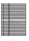
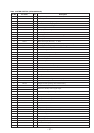
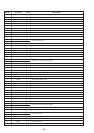
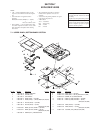

– 49 – – 50 – – 52 –– 51 –
MZ-R50
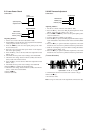
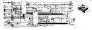
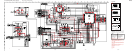
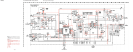
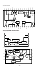
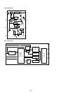
6-5. SCHEMATIC DIAGRAM – MAIN (1/3) SECTION –
r
Refer to page 61 for IC Block Diagram.
Note:
• All capacitors are in µF unless otherwise noted. pF: µµF
50 WV or less are not indicated except for electrolytics
and tantalums.
• All resistors are in Ω and
1
/
4
W or less unless otherwise
specified.
Note: Note:
The components identi- Les composants identifiés
fied by mark ! or dotted par une marque ! sont cri-
line with mark ! are cri- tiques pour la sécurité.
tical for safety. Ne les remplacer que par
Replace only with part une piéce portant le
number specified. numéro spécifié.
• A : B+ Line.
• Power voltage is dc 6V and fed with regulated dc power
supply from external power voltage jack (J901).
• Voltages and waveforms are dc with respect to ground
under no-signal (detuned) conditions.
no mark : PB
( ) : REC
• Voltages are taken with a VOM (Input impedance 10 MΩ).
Voltage variations may be noted due to normal produc-
tion tolerances.
• Waveforms are taken with a oscilloscope.
Voltage variations may be noted due to normal produc-
tion tolerances.
• Circled numbers refer to waveforms.
• Signal path.
E : PB
a : REC
1
2
3
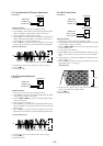
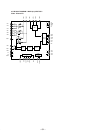
IC501 #•
r
WAVEFORMS
4
1.1Vp-p
Approx. 0.5Vp-p
2.8Vp-
p
13.4msec
2.8Vp-
p
22.5MHz
VOLT/DIV : 0.5V AC
TIME/DIV : 1µsec
IC501 @ª
VOLT/DIV : 0.1V AC
TIME/DIV : 1msec
IC503 !¡
VOLT/DIV : 1V AC
TIME/DIV : 5msec
IC503 !
VOLT/DIV : 1V AC
TIME/DIV : 20nsec