


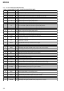
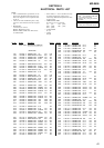
39
MZ-E505
Pin No.
Pin Name
I/O Description
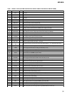
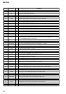
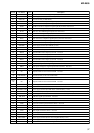
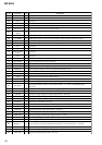
204 XPD ADA O Power supply control signal output terminal Not used
205 XCS LCD O Chip select signal output terminal Not used
206 LCD STB O Strobe signal output terminal Not used
207 OPR LED G H O Not used
208 REC OPR LED O LED ON/OFF control signal output terminal for REC display Not used
209 OPR LED G L O Not used
210 TSB SLV CHK O TSB slave detection signal output terminal Not used
211 OPR LED R H O Not used
212 OPR LED R L O Not used
213 MCUVSS1
—
Ground terminal (for the microcomputer block)
214 GND SW O GND changeover control signal output terminal Not used
215 XOPT CTL O Power supply ON/OFF control signal output terminal for DIN PD drive Not used
216 CS RTC O Chip select signal output terminal Not used
217 VG CTL O Not used
218 MUTE O Analog muting control signal output to the headphone amp “H”: muting ON
219 XCS NV O Chip select signal output to EEPROM
220
XRST MTR
DRV
O Reset control signal output to the motor driver
221 XRF RST O Reset control signal output to RF amp
222 MCUVDD3
—
Power supply terminal (for the microcomputer block) (+1.5V)
223 SPDL MON I Spindle servo monitor signal input from the motor driver
224 XAVLS I Input terminal for AVLS switch detection signal Not used
225, 226 JOG A, B I Jog dial pulse input terminal Not used
227 XHOLD SW I HOLD switch input terminal “L”: hold ON, “H”: hold OFF
228 SYNC REC I SYNCHRO REC switch input terminal “L”: OFF, “H”: ON Not used
229 TSB SSB CTL O TSB/SSB changeover control signal output terminal Not used
230 PROTECT I
Detection input terminal of the record check claw
“L”: recording possible condition, “H”: protect Not used
231 FLASHVDD
—
Power supply terminal (for the internal FLASH ROM) (+2.3V)
232 FLASHVSS
—
Ground terminal (for the internal FLASH ROM)
233 SLD MON I Sled servo monitor signal input from the motor driver
234 VLON O Power supply control signal output for the laser diode drive to the power control
235 SLEEP O System sleep control signal output to the power control “H”: sleep ON
236 FFCLR O Input latch output for the start switching to the power control
237 CHG GAIN O Charge gain control signal output terminal Not used
238 CHG O Charge ON/OFF control signal output terminal “H”: charge ON Not used
239 NC O Not used
240 XHP STBY O Power supply control signal output for the headphone amp
241 MIFVDD3
—
Power supply terminal (for the microcomputer I/F block) (+1.9V)
242 MIFVSS2
—
Ground terminal (for the microcomputer I/F block)
243 TEST2 I Input terminal for the main test (normally open)
244 NC
—
Not used