


– 49 –
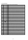
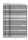
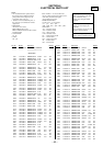
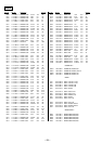
Pin No. Pin Name I/O Pin Description
43 XRST I
System reset signal input from the MPC18A31FTA (IC901) “L”: reset
For several hundreds msec. after the power supply rises, “L” is input, then it changes to “H”
44 VSS — Ground terminal
45 XTAL O Main system clock output terminal (16.9344 MHz)
46 EXTAL I Main system clock input terminal (16.9344 MHz)
47 VDD — Power supply terminal (+2.4 V)
48 TSB SLV CTL I/O Two-way control signal bus with TSB slave circuit Not used (open)
49 SPDL START SW O Spindle servo start switching signal output to the analog switch (IC504, 505)
50 OPEN CLOSE SW I
Upper panel open/close detect switch (S801) input terminal (A/D input)
“L”: upper panel close, “H”: upper panel open
51 XSHOCK I Recording shock detect signal input from the CXD2660GA (IC502)
52 FOK I Focus OK signal input from the CXD2660GA (IC502) “H”: is input when focus is on (“L”: NG)
53 SQSY I
Subcode Q sync (SCOR) input from the CXD2660GA (IC502)
“L” is input every 13.3 msec Almost all, “H” is input
54 DQSY I
Digital In U-bit CD format subcode Q sync (SCOR) input from the CXD2660GA (IC502)
“L” is input every 13.3 msec Almost all, “H” is input
55 XINT I Interrupt status input from the CXD2660GA (IC502)
56 T.MARK I T MARK switch (S803) input terminal
57 REC WBL SW O Stable control signal is output when recording
58 SERON O Series power supply control signal output to the MPC18A31FTA (IC901)
59 XCHG O Charge control signal output to the MPC18A31FTA (IC901)
60 XTEST I Setting terminal for the test mode “L”: test mode, normally: fixed at “H”
61 SET CODE0 I Destination setting terminal for the test mode
62 SET CODE1 I Destination setting terminal for the test mode Not used (open)
63 SET CODE2 I Destination setting terminal for the test mode
64 REG CTL PWM O Synchronizing external clock signal output to the MPC18A31FTA (IC901)
65 VRM PWM O VREM power supply voltage control PWM signal output to the MPC18A31FTA (IC901)
66 VC PWM O System power supply voltage control PWM signal output to the MPC18A31FTA (IC901)
67 SPDL PWM O Spindle servo drive voltage control PWM signal output to the MPC17A56FTA (IC901)
68 XIC RST O
Reset signal output to the A/D, D/A converter (IC301), SN761056ADBT (IC501) and
CXD2660GA (IC502) “L”: reset
69 REC LED O REC LED drive signal output terminal Not used (open)
70 SI1 I Joint text data input from the remote commander with headphone
71 SO1 O Joint text data output to the remote commander with headphone Not used (open)
72 SCK1 O
Joint data communication clock output to the remote commander with headphone
Not used (open)
73 XHOLD SW I HOLD switch (S804) input terminal “L”: hold on, “H”: hold off
74 VDD — Power supply terminal (+2.4 V)
75 TEX I Sub system clock input terminal Not used (open)
76 TX O Sub system clock output terminal Not used (open)
77 VSS — Ground terminal
78 VBKAN I Sub power supply input terminal
79 S MON I Servo signal monitor input from the SN761056ADBT (IC501) (A/D input)
80 VB MON I Un-regulator power supply voltage monitor input terminal (A/D input)
81 CHG MON I Rechargeable battery voltage monitor input from the MPC18A31FTA (IC901) (A/D input)
82 VREF MON I Reference voltage monitor input from the SN761056ADBT (IC501) (A/D input)
83 WK DET I Set key starting detect signal input terminal (A/D input)
84 HALF LOCK SW I Open knob detect switch (S802) input terminal “L”: normal position, “H”: open knob slid
85 RMC KEY I Remote commander with headphone key input terminal (A/D input)
86 SET KEY 1 I Set key input terminal (A/D input) (x, >, ., VOL +/– keys input)