


– 45 –
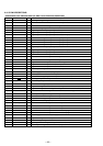
Pin No. Pin Name I/O Pin Description
1 VDC0 — Power supply terminal (+1.8 V) (for internal logic)
2 MNT0 I/O Not used (open)
3 MNT1 O Recording shock detect signal output to the system controller (IC801)
4 MNT2 O Off track signal output to the SN761056ADBT (IC501) and system controller (IC801)
5 MNT3 O
Focus OK signal output to the system controller (IC801)
“H”: is output when focus is on (“L”: NG)
6 SWDT I Serial data input from the system controller (IC801)
7 SCLK I (S) Serial clock signal input from the system controller (IC801)
8 XLAT I (S) Serial data latch pulse input from the system controller (IC801)
9 VSC0 — Ground terminal (for internal logic)
10 SRDT O (3) Serial data output to the system controller (IC801)
11 SENS O (3) Internal status (SENSE) output to the system controller (IC801)
12 XRST I (S) Reset signal input from the system controller (IC801) “L”: reset
13 SQSY O
Subcode Q sync (SCOR) output the system controller (IC801)
“L” is output every 13.3 msec Almost all, “H” is output
14
DQSY
O
Digital In U-bit CD format subcode Q sync (SCOR) output to the system controller (IC801)
(MTFLGL) “L” is output every 13.3 msec Almost all, “H” is output
15 WRPWR I
Laser power selection signal input from the system controller (IC801)
“L”: playback mode, “H”: recording mode
16 XINT O Interrupt status output to the system controller (IC801)
17 TX I
Recording data output enable signal input from the system controller (IC801)
Writing data transmission timing input
18 VDIO0 — Power supply terminal (+2.4 V) (for I/O)
19 OSCI I System clock (512Fs=22.5792 MHz) input terminal
20 OSCO O System clock (512Fs=22.5792 MHz) output terminal
21 VSIO0 — Ground terminal (for I/O)
22 to 29 NC — Not used (open)
30 VSC1 — Ground terminal (for internal logic)
31 XTSL I
Input terminal for the system clock frequency setting
“L”: 45.1584 MHz, “H”: 22.5792 MHz (fixed at “H” in this set)
32 XCS_DSP I Chip select signal input from the system controller (IC801)
33 DIN1 I Digital audio signal input terminal when recording mode
34 DOUT O Digital audio signal output terminal when playback mode Not used (open)
35 DT72 O Not used (open)
36, 37 VDC1, VDC2 — Power supply terminal (+1.8 V) (for internal logic)
38 DATAI I Serial data input terminal Not used (fixed at “L”)
39 LRCKI I
L/R sampling clock signal (44.1 kHz) input terminal
“L”: Rch, “H”: Lch Not used (fixed at “L”)
40 XBCKI I Serial input/output data bit clock signal (2.8224 MHz) input terminal Not used (fixed at “L”)
41 ADDT I Recording data signal input from the A/D, D/A converter (IC301)
42 DADT O Playback data signal output to the A/D, D/A converter (IC301)
43 LRCK O L/R sampling clock signal (44.1 kHz) output to the A/D, D/A converter (IC301)
44 VSC2 — Ground terminal (for internal logic)
45 XBCK O Serial input/output data bit clock signal (2.8224 MHz) output to the A/D, D/A converter (IC301)
46 FS256 O Clock signal (11.2896 MHz) output to the A/D, D/A converter (IC301) (X' tal system)
47 to 52
A03, A04, A02,
O Address signal output to the external D-RAM Not used (open)
A05, A01, A06
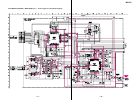
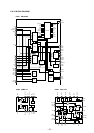
• MAIN BOARD IC502 CXD2660GA
(DIGITAL SIGNAL PROCESSOR, DIGITAL SERVO SIGNAL PROCESSOR, EFM/ACIRC ENCODER/DECODER,
SHOCK PROOF MEMORY CONTROLLER, ATRAC ENCODER/DECODER, 16M BIT D-RAM)
* I (S) stands for schmitt input, I (A) for analog input, O (3) for 3-state output, and O (A) for analog output in the column I/O