


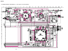

– 48 –
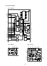
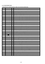
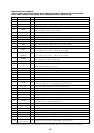
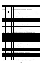
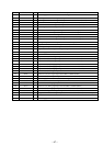
Pin No. Pin Name I/O Pin Description
1 SYNC REC I SYNCHRO REC switch (S801) input terminal “L”: off, “H”: on
2 OFTRK I Off track signal input from the CXD2660GA (IC502)
3 PROTECT I
Rec-proof claw detect input from the protect detect switch (S806)
“L”: recording possible, “H”: protect
4 PAUSE KEY I Set pause key input terminal
5TXO
Recording data output enable signal output to the CXD2660GA (IC502)
Writing data transmission timing output
6 SENSE I Internal status (SENSE) input from the CXD2660GA (IC502)
7 WRPWR O
Laser power select signal output to the CXD2660GA (IC502)
“L”: playback mode, “H”: recording mode
8 XLAT O Serial data latch pulse output to the CXD2660GA (IC502)
9 XCS DSP O Chip select signal output to the CXD2660GA (IC502)
10 CS RTC O Not used (open)
11 SI0 I
Serial data input from the A/D, D/A converter (IC301), CXD2660GA (IC502), EEPROM
(IC802) and switch & liquid crystal display module unit
12 SO0 O
Serial data output to the A/D, D/A converter (IC301), CXD2660GA (IC502), EEPROM
(IC802) and switch & liquid crystal display module unit
13 SCK0 O
Serial clock signal output to the A/D, D/A converter (IC301), CXD2660GA (IC502),
EEPROM (IC802) and switch & liquid crystal display module unit
14 XGUM ON I Not used (open)
15 VSS — Ground terminal
16 VDD — Power supply terminal (+2.4 V)
17 XOUT O Not used (open)
18 BEEP O Beep sound control signal input terminal
19 RMC DTCK I/O TSB serial communication data input/output terminal for remote commander with headphone
20 XCS LCD O Chip select signal output to the liquid crystal display
21 LCD STB O Strobe signal output to the liquid crystal display
22 LCD RST O Reset control signal output to the liquid crystal display
23 XHP STBY O
Standby on/off control signal output to the line/headphone amplifier (IC303)
“L”: standby mode, “H”: amplifier on
24 CLV U O Spindle servo (U) drive signal input from the MPC17A56FTA (IC601)
25 CLV V O Spindle servo (V) drive signal input from the MPC17A56FTA (IC601)
26 CLV W O Spindle servo (W) drive signal input from the MPC17A56FTA (IC601)
27 MODE1 O Power supply control signal output for over write head drive to the MPC18A21MTB (IC603)
28 MODE2 O Power supply control signal output for over write head drive to the MPC18A21MTB (IC603)
29 MODE3 O Power supply control signal output for over write head drive to the MPC18A21MTB (IC603)
30 HD CON 1 O Over write head control signal output to the MPC18A21MTB (IC603)
31 HD CON 2 O Over write head control signal output to the MPC18A21MTB (IC603)
32 XREC MODE O Not used (open)
33 LD ON O Laser diode on/off control signal output terminal “L”: laser off, “H”: laser on Not used (open)
34 TSB SLV ON I TSB slave detect signal input terminal
35 SLD MON 1 I Sled servo timing signal input from the MPC17A56FT (IC601)
36 PD S0 O PD IC mode switching signal output to the optical pick-up block
37 REG CTL CLK O Synchronizing external clock signal output terminal Not used (open)
38 PD S1 O PD IC mode switching signal output to the optical pick-up block
39 FFCLR O Input latch output for starting signal to the MPC18A31FTA (IC901)
40 SLEEP O System sleep control signal output to the MPC18A31FTA (IC901) “H”: sleep on
41 TSB EDGE I TSB slave edge detect signal input terminal
42 GND SW O Ground line switching signal output terminal
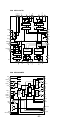
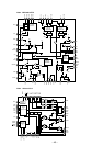
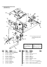
• MAIN BOARD IC801 CXR701080-010GA (SYSTEM CONTROLLER)