


4
CDX-MP40
TABLE OF CONTENTS
1. GENERAL
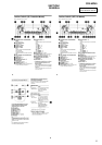
Location of Controls (US, Canadian Model) .......................... 5
Location of Controls (AEP, UK Model).................................. 5
Connections (US, Canadian Model)........................................ 6
Connections (AEP, UK Model) ............................................... 7
2. DISASSEMBLY
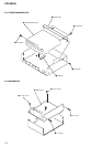
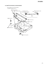
2-1. Sub Panel Assy (CD)........................................................... 9
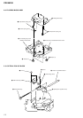
2-2. CD Mechanism Block .......................................................10
2-3. Main Board ....................................................................... 10
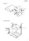
2-4. Heat Sink ...........................................................................11
2-5. Chassis (T) Sub Assy ........................................................ 11
2-6. Lever Section.....................................................................12
2-7. Servo Board.......................................................................12
2-8. Shaft Roller Assy, Load Sw Board....................................13
2-9. Floating Block Assy ..........................................................14
2-10. Optical Pick-up Block .......................................................14
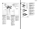
3. DIAGRAMS
3-1. IC Pin Descriptions ...........................................................15
3-2. Circuit Boards Location .................................................... 20
3-3. Block Diagram –CD Section–...........................................21
3-4. Block Diagram –Main Section–........................................ 22
3-5. Block Diagram –Display Section–.................................... 23
3-6. Printed Wiring Boards –CD Mechanism Section–............24
3-7. Schematic Diagram –CD Mechanism Section (1/2)– ....... 26
3-8. Schematic Diagram –CD Mechanism Section (2/2)– ....... 27
3-9. Printed Wiring Boards –Main Section– ............................ 28
3-10. Schematic Diagram –Main Section (1/2)– ........................29
3-11. Schematic Diagram –Main Section (2/2)– ........................30
3-12. Printed Wiring Board –Relay Section– ............................. 31
3-13. Printed Wiring Board –Key Section
(US, Canadian Model)– ............... 32
3-14. Schematic Diagram –Relay, Key Section
(US, Canadian Model)–..................33
3-15. Printed Wiring Board –Key Section
(AEP, UK Model)– ...................... 34
3-16. Schematic Diagram –Relay, Key Section
(AEP, UK Model)– .........................35
3-17. IC Block Diagrams............................................................36
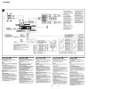
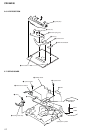
4. EXPLODED VIEWS
4-1. Chassis Section ................................................................. 38
4-2. Front Panel Section ...........................................................39
4-3. CD Mechanism Section (1) ...............................................40
4-4. CD Mechanism Section (2) ...............................................41
4-5. CD Mechanism Section (3) ...............................................42
5. ELECTRICAL PARTS LIST ........................................43