


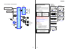
23 23
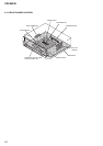
CDX-MP40
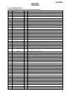
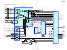
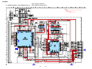
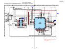
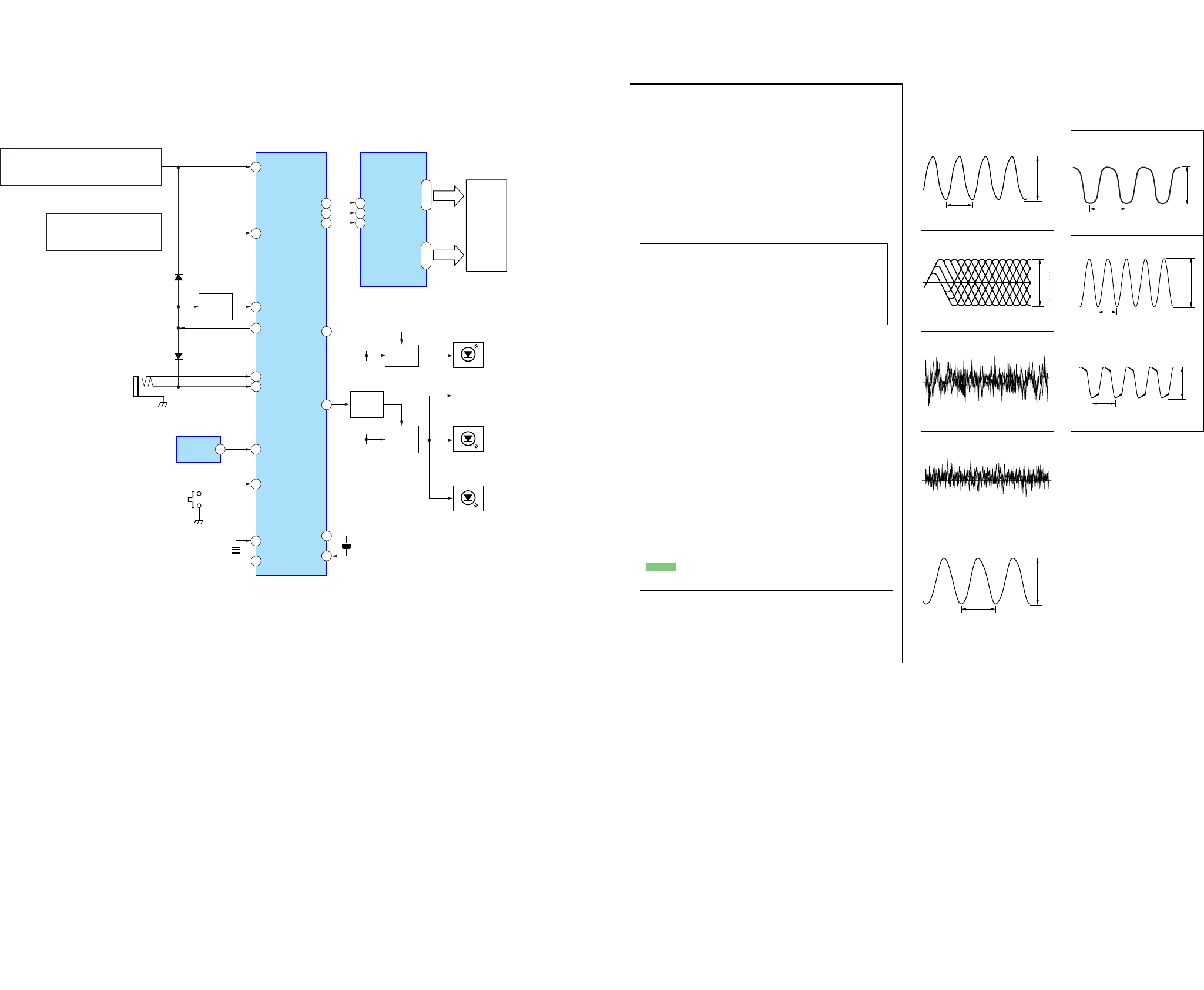
3-5. BLOCK DIAGRAM — DISPLAY SECTION —
Note:
The components identi-
fied by mark 0 or dotted
line with mark 0 are criti-
cal for safety.
Replace only with part
number specified.
Note:
Les composants identifiés par
une marque 0 sont critiques
pour la sécurité.
Ne les remplacer que par une
piéce portant le numéro
spécifié.
THIS NOTE IS COMMON FOR PRINTED WIRING
BOARDS AND SCHEMATIC DIAGRAMS.
(In addition to this, the necessary note is
printed in each block.)
for schematic diagram:
• All capacitors are in µF unless otherwise noted. pF: µµF
50 WV or less are not indicated except for electrolytics
and tantalums.
• All resistors are in Ω and
1
/
4
W or less unless otherwise
specified.
•%: indicates tolerance.
•
f
: internal component.
• C : panel designation.
• A : B+ Line.
• Power voltage is dc 14.4V and fed with regulated dc power
supply from ACC and BATT cords.
•Voltages are taken with a VOM (Input impedance 10 MΩ).
Voltage variations may be noted due to normal produc-
tion tolerances.
•Waveforms are taken with a oscilloscope.
Voltage variations may be noted due to normal produc-
tion tolerances.
• Circled numbers refer to waveforms.
• Signal path.
F : FM
f : AM/MW/LW
J : CD
c : CD-R/RW (MP3)
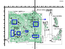
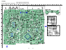
for printed wiring boards:
• X : parts extracted from the component side.
• Y : parts extracted from the conductor side.
• x : parts mounted on the conductor side.
•
a
: Through hole.
• : Pattern from the side which enables seeing.
(The other layer’s patterns are not indicated.)
Caution:
Pattern face side: Parts on the pattern face side seen from the
(Side B) pattern face are indicated.
Parts face side: Parts on the parts face side seen from the
(Side A) parts face are indicated.
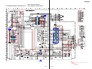
• Waveforms
— SERVO Board —
(MODE: CD PLAY)
—
MAIN Board —
1
2
3
4
2.8 Vp-p
59 ns
1V/DIV,20ns/DIV
5
1.2 Vp-p
82 ns
1V/DIV,40ns/DIV
Approx. 200m Vp-p
Approx. 300m Vp-p
100mV/DIV,20µs/DIV
100mV/DIV,20µs/DIV
500mV/DIV,1µs/DIV
1.7 Vp-p
IC1 wd (XTAL)
IC1 uj (RFO)
IC1 oa (FEO)
IC1 od (TEO)
IC3 yd (XTAL)
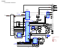
6
7
8
2V/DIV,40ns/DIV
3.2 Vp-p
54 ns
2V/DIV,20µs/DIV
3.8 Vp-p
30.5
µ
s
2V/DIV,100ns/DIV
230 ns
5.5 Vp-p
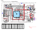
IC601 4 (OSCD)
IC801 qs (OSCOUT)
IC801 qh (XOUT)
Q803
KEY
DETECT
CNP801
(REMOTE IN)
IC951(US,Canadian MODEL)
IC971(AEP,UK MODEL)
X802
32.768kHz
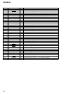
15
16
12
13
5
18
20
19
4
26
91
98
6
292
IC801 (2/2)
SYSTEM CONTROL
IC901
LCD DRIVER
(US,Canadian MODEL)
(AEP,UK MODEL)
KEY IN0
DATA
CLK
CE
LCDSO
LCDCKO
LCDCE
Q919
ILL ON
SWITCH
Q918
ILL B+
SWITCH
KEY IN1
KEY ACK
XKEYON
RC IN1
RC IN0
SIRCS
34
NOSE SW
XIN
XOUT
OSC OUT
92
ILLON
75
DOOR
IND
BATT
ILL B+
OSC IN
X801
18.432MHz
AEP,UK:LED933,934
US,CND:LED910,911
LCD BACK
LIGHT
78
77
76
COM1
COM4
LCD901
LIQUID
CRYSTAL
DISPLAY
D809
D807
()
AEP,UK:LED903,911,951-954,LSW901(2/2),
904(2/2)-910(2/2),912(2/2)-922(2/2)
US,CND:LED901-906,LSW901(2/2)-917(2/2)
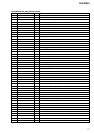
KEY
ILLUMINATION
(
)
65
|
68
1
I
64
S1
I
S64
|
REMOTE
CONTROL
RECEIVER
AEP,UK:S911,LSW912(1/2)-922(1/2)
US,CND:S902,LSW908(1/2)-917(1/2)
FUNCTION SWITCH
AEP,UK:S902,903,931,LSW901(1/2),904(1/2)-910(1/2)
US,CND:S901,903,931,LSW901(1/2)-907(1/2)
FUNCTION SWITCH
DOOR IND
SW
BATT
LED930,931
S802
(NOSE DET)
Q923,924