


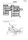
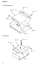
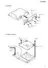
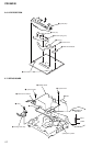
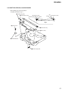
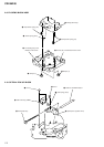
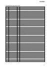
17
CDX-MP40
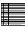
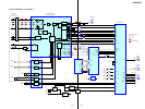
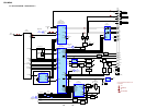
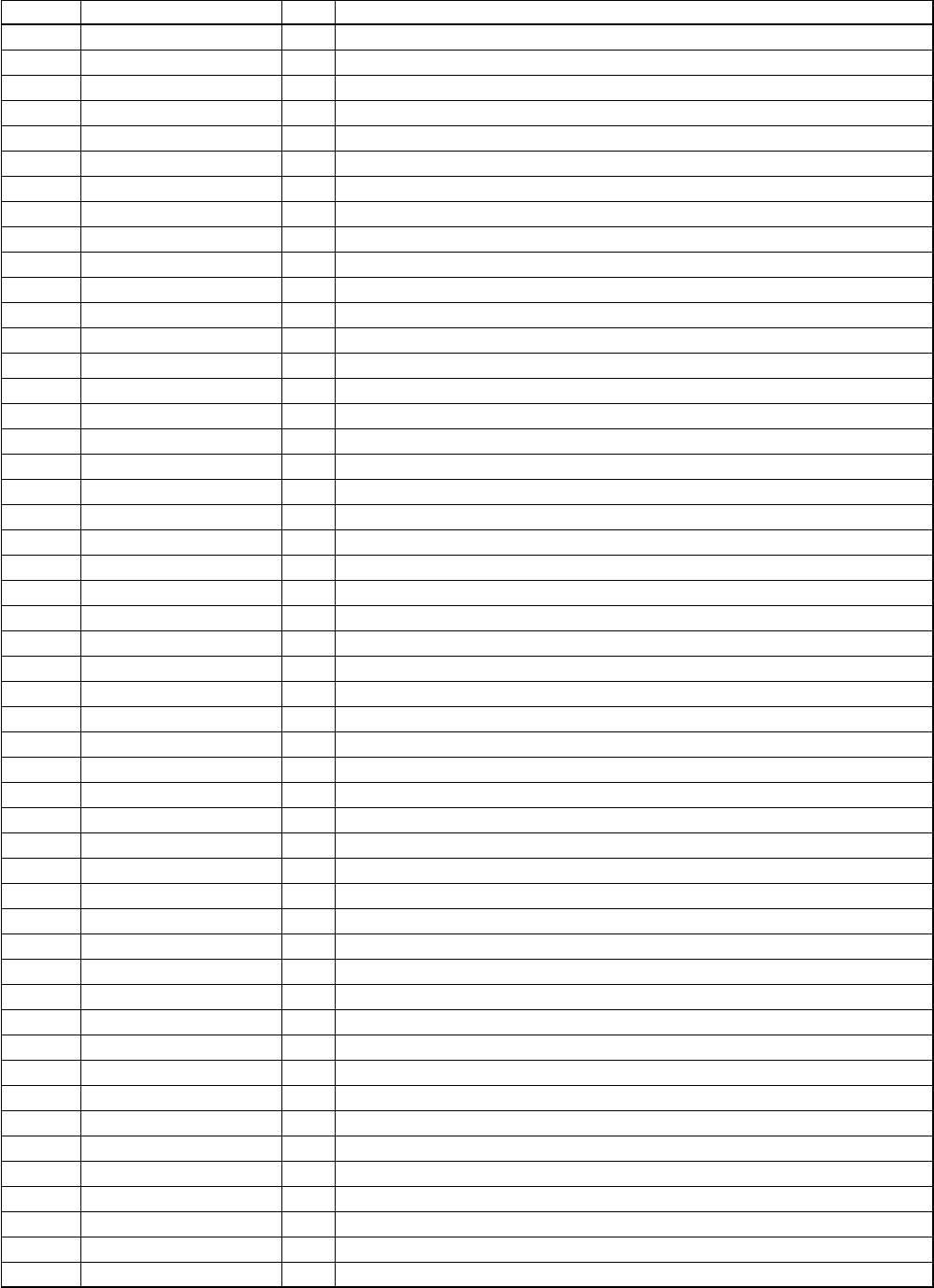
• IC5 CXD9684R-005 (DSP) (SERVO BOARD)
Pin No. Pin Name I/O Pin Description
1 /RESET I Reset input pin “L”: reset
2MIMD I Microcomputer interface mode selection input “H”: I2C, “L”: TSB
3, 4 AD0, AD1 O External SRAM address signal output
5 MIDIO (I2C_SDA) I/O Serial data input/output
6 MICK (I2C_SCL) I Serial clock input
7 AD2 O External SRAM address signal output
8 VDDT (3.3V) — Power supply (3.3 V) for digital circuit
9 SDO O Data output
10, 11 AD3, AD4 O External SRAM address signal output
12 SDI0 I Data input 0
13 BCKIA I Bit clock input A
14 LRCKIA I LR clock input A
15 AD5 O External SRAM address signal output
16 CE O External SRAM chip enable signal output
17 OE O External SRAM output enable signal output
18 VDD (2.5V) — Power supply pin (2.5 V) for digital circuit
19 STANDBY I Standby mode control signal input “H”: STB, “L”: normal
20 VSS (2.5VGND) — Ground pin for digital circuit
21 VSSL (2.5VGND) — Ground pin for DAC Lch
22 VRAL — Reference voltage pin for DAC Lch
23 LO O DAC Lch signal output (Open)
24 VDAL (2.5V) — Power supply pin (2.5 V) for DAC Lch
25 VDAR (2.5V) — Power supply pin (2.5 V) for DAC Rch
26 RO O DAC Rch signal output (Open)
27 VRAR — Reference voltage pin for DAC Rch
28 VSSR (2.5VGND) — Ground pin for DAC Rch
29 TESTP I Pin for test “H”: test mode, “L”: normal (fixed at “L”)
30 CKS I VCO selection input “H”: VCO, “L”: X1 input
31 – 34 AD12 to AD9 O External SRAM address signal output
35 VDDT (3.3V) — Power supply pin (3.3 V) for digital circuit
36 – 38 AD8 to AD6 O External SRAM address signal output
39 REQ O Interrupt request signal output to the CD master control
40 VSS — Ground pin for digital circuit
41, 42 AD13, AD14 O External SRAM address signal output
43 WR O External SRAM write signal output
44, 45 AD16, AD15 O External SRAM address signal output
46, 47 IO0, IO1 I/O External SRAM data input/output
48 VSS — Ground pin for digital circuit
49 – 51 IO2 to IO4 I/O External SRAM data input/output
52 VDD (2.5V) — Power supply pin (2.5 V) for digital circuit
53 – 55 IO5 to IO7 I/O External SRAM data input/output
56 VSSP — Ground pin for VCO circuit
57 PDO O PLL phase error detection signal output
58 VCOI I VCO control voltage input
59 VDDP — Power supply pin for VCO circuit
60 XRDE I/O External clock input, audio clock output Not used. (Open)
61 VDDX (2.5V) — Power supply pin for oscillation circuit
62 XI I Resonator pin
63 XO O Resonator pin
64 VSSX — Ground pin for oscillation circuit