


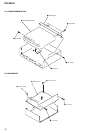
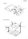
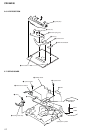
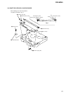
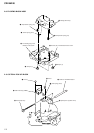
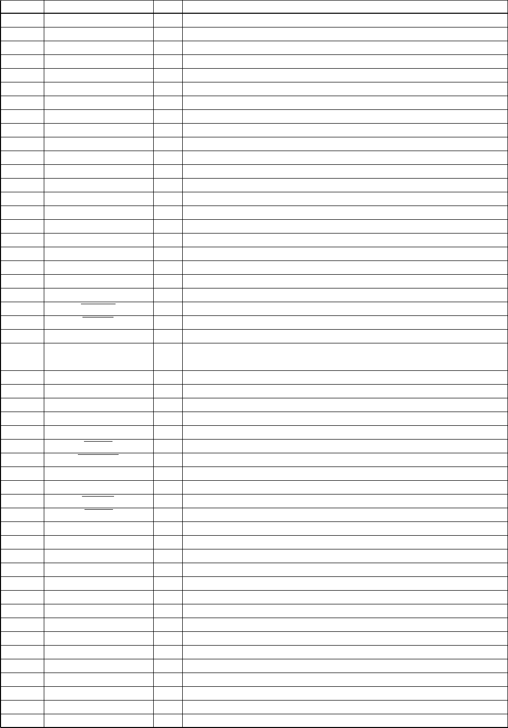
18
CDX-MP40
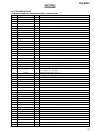
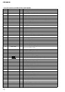
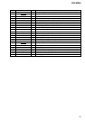
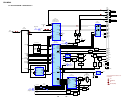
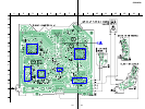
• IC801 MN101C49KSJ (SYSTEM CONTROL) (MAIN BOARD)
Pin No. Pin Name I/O Pin Description
1VREF– — Power supply pin for A/D converter
2 VSM I S-meter voltage detection signal input from the tuner unit (TU601)
3NIL I Not used. (Connected to ground.)
4 KEYIN1 I Key signal input
5 KEYIN0 I Key signal input
6 RC_IN0 I Rotary commander key signal input from the remote-in jack
7QUALITY I Noise detection signal input (AEP, UK model)/Connected to ground. (US, Canadian model)
8 DST SEL I Destination setting pin (US, Canadian model)
9NIL I Not used. (Connected to ground.)
10 VREF+ — Power supply pin for A/D converter
11 VDD — Power supply pin
12 OSCOUT O High speed clock output (18.43 MHz)
13 OSCIN I High speed clock input (18.43 MHz)
14 VSS — Ground pin
15 XIN I Low speed clock input (32.768 kHz)
16 XOUT O Low speed clock output (32.768 kHz)
17 MMOD — Memory mode selection input “L”: single chip mode (connected to ground)
18 LCDSO O Serial data output to the LCD driver
19 LCDCE O Chip enable signal output to the LCD driver
20 LCDCKO O Serial clock output to the LCD driver
21 – 23 NCO O Not used. (Open)
24 SYSRST O System reset signal output
25 BUSON O Bus on signal output to the bus interface
26 KEYACK I Key acknowledge detection signal input
27 DAVN (NIL) I
RDS data block sync detection signal input (AEP, UK model)/Connected to
ground. (US, Canadian model)
28 BU_IN I Back up power supply detection signal input
29 SIRCS I Remote control signal input from the remote control receiver
30 TUATT IN I ATT control signal input from tuner unit.
31 NIL I Not used. (Connected to ground.)
32 NIH I Not used. (Connected to power supply.)
33 RESET I Microcomputer reset signal input from the reset IC
34 NOSE SW I Front panel with/without detection signal input “L”: panel with
35 BEEP O Beep signal output to the power amplifier
36 NCO O Not used. (Open)
37 TESTIN I Test mode detection signal input
38 ACCIN I Accessory power supply detection signal input
39 NCO O Not used. (Open)
40 TELATT I TEL ATT detection signal input
41 NIH I Fixed at “H”.
42 BUSSO O Sony_Bus serial data output to the bus interface IC
43 BUSSI I Sony_Bus serial data input from the bus interface IC
44 BUSCKO O Sony_Bus serial clock output to the bus interface IC
45 I2CSIO I/O I2C bus serial data input/output
46 NCO O Not used. (Open)
47 I2CCKO O I2C bus serial clock output
48 NCO O Not used. (Open)
49 NCO O Not used. (Open)
50 POW_ON O System power supply control signal output
51 – 66 NCO O Not used. (Open)
67 ATT O System ATT control signal output
68 NCO O Not used. (Open)