


15
CDX-MP40
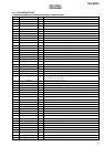
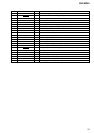
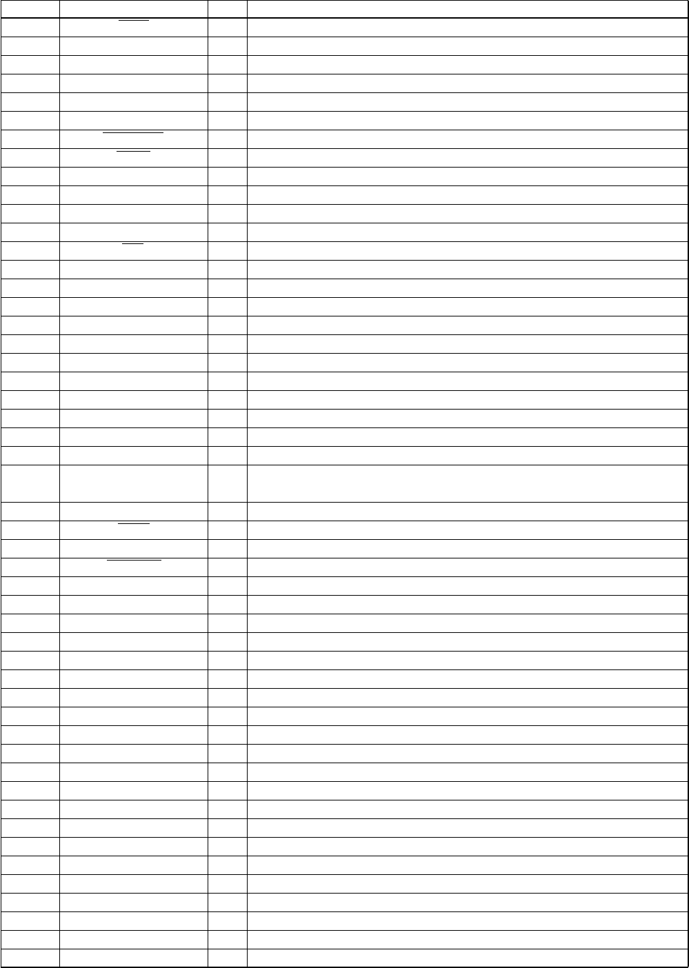
3-1. IC PIN DESCRIPTIONS
• IC3 HD6432238RWN35TEI (CD MASTER CONTROL) (SERVO BOARD)
Pin No. Pin Name I/O Pin Description
1 TEST I Test mode selection pin Not used. (Open)
2 DECXRST O Reset signal output to the DSP IC “L”: reset
3 DECSTBY O Standby mode control signal output to the DSP IC “H”: standby
4 – 7 NC O Not used. (Open)
8PH3 I CD PH3 photo sensor detection signal input Not used. (Open)
9 INSW/PH2 I CD mechanism disc in switch detection signal input
10 LIMIT_SW I CD mechanism in-limit switch detection signal input
11 D_SW I CD mechanism down switch detection signal input
12 CVCC — System power supply pin (+3.3 V)
13 NC O Not used. (Open)
14 VSS — Ground pin
15 NC O Not used. (Open)
16 PH1 I CD PH1 photo sensor detection signal input Not used. (Open)
17 EJECT O CD mechanism loading motor control signal output (eject operation)
18 LOAD O CD mechanism loading motor control signal output (load operation)
19 – 26 NC O Not used. (Open)
27 FLAG I Correction unable detection signal input
28 RFOK I RFOK signal input from the servo IC
29, 30 NC O Not used. (Open)
31 TXD O UART TXD PC connection output Not used. (Open)
32 RXD I UART RXD PC connection input Not used. (Open)
33 XTALEN O Crystal oscillation control signal output to the servo IC
34 TSTB O CD text parameter strobe signal output to the servo IC
35 STB O Data strobe signal output to the servo IC
36 A0 O
Command/parameter identification signal output to the servo IC
“L”: command, “H”: parameter
37 CD_RST O Reset signal output to the servo IC
38 PACK I CD text pack sync signal input from the servo IC
39 NC O Not used. (Open)
40 SELF_SW I CD mechanism self load position detection switch signal input
41 NC O Not used. (Open)
42 AVSS — Ground for A/D converter
43, 44 NC O Not used. (Open)
45, 46 NC I Not used. (Open)
47 KEY0 I Key switch signal input in the test mode Not used. (Open)
48 KEY1 I Mode switch signal input in the test mode Not used. (Open)
49 – 52 NC I Not used. (Open)
53 AVREF — Reference voltage for A/D converter
54 AVCC — Power supply for A/D converter
55 MD0 — CPU operation mode setting pin Connecting to +3.3 V in this set.
56 MD1 — CPU operation mode setting pin Connecting to +3.3 V in this set.
57 X1A — Sub clock oscillator terminal Not used. (Open)
58 X0A — Sub clock oscillator terminal Not used. (Open)
59 RSTX I Microcomputer reset signal input
60 NMI — Not used. (Fixed at “H”)
61 STBY — Not used. (Fixed at “H”)
62 VCC — Power supply pin (+3.3 V)
63 XTAL — Main clock oscillator pin (12.288 MHz)
64 VSS — Ground pin
65 XTEAL — Main clock oscillator pin (12.288 MHz)
66 FWE I Flash write enable signal input
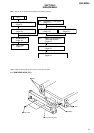
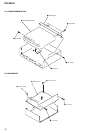
SECTION 3
DIAGRAMS