


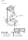
34
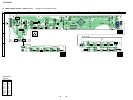
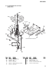
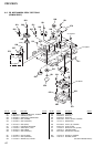
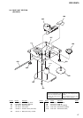
CDP-CE575
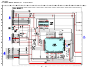
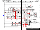
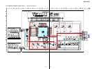
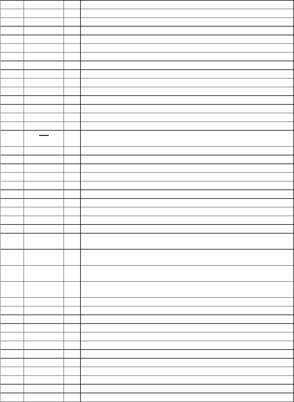
• MAIN BOARD IC301 CXP84648-085Q (SYSTEM CONTROLLER)
Pin No. Pin Name I/O Description
1 to 4 A3 to A6 O
Address signal output to the static RAM (IC302)
5
GND — Ground terminal
6 to 13 D0 to D7 I/O Two-way data bus with the static RAM (IC302)
14 CE O Chip select signal output to the static RAM (IC302)
15 to 18 NC
— Not used (open)
19
WE O Write enable signal output to the static RAM (IC302)
20 LOAD OUT O Loading motor (M10) drive signal output to the BA6780 (IC11)
21 LOAD IN O Loading motor (M10) drive signal output to the BA6780 (IC11)
22
FL CLK O Serial data transfer clock signal output to the FL driver (IC801)
23
FL DATA O Serial data output to the FL driver (IC801)
24
FL RST O Reset signal output to the FL driver (IC801)
25 to 27 A13, A14, A7 O
Address signal output to the static RAM (IC302)
28
DSENS I Detect signal input from the disc sensor (D11)
29
NC — Not used (open)
30
RST I
System reset signal input from the reset signal generator (IC603) “L”: reset
For several hundreds msec. after the power supply rises, “L” is input, then it changes to “H”
31
EXTAL I Main system clock input terminal (10 MHz)
32
XTAL O Main system clock output terminal (10 MHz)
33
VSS — Ground terminal
34
TX O Sub system clock output terminal Not used (open)
35
TEX I Sub system clock input terminal Not used (fixed at “L”)
36
AVSS — Ground terminal (for A/D converter)
37
AVREF I Reference voltage input terminal (+5V)
38 NC — Not used (open)
39 VERSION I Model Destination setting terminal
40 ADJ I Setting terminal for the test mode
41 KEY4 I
Key input terminal (A/D input) (S941 to S845) FADER, PEAK SEARCH, CLEAR, CHECK,
EDIT keys input
42 KEY3 I
Key input terminal (A/D input) (S831 to S838) DISC 5, DISC 4, DISC 3, DISC 2, DISC 1,
CONTINUE, SHUFFLE, PROGRAM keys input
43 KEY2 I
Key input terminal (A/D input) (S821 to S827) MEGA CONTROL, X-FADER NO DELAY,
MENU, m (AMS–), M (AMS+), TIME/TEXT, REPEAT keys input
44 KEY1 I
Rotary encoder key input terminal (A/D input) (S801, S811 to S815) l AMS L (DISC)
PUSH ENTER, H, X, s, EX-CHANGE, DISC SKIP keys input
45 NC — Not used (open)
46
TSENS I Detect signal input from the table sensor (D10)
47 FLT O Serial data latch pulse output to the FL driver (IC801)
48 CLK O Serial data transfer clock signal output to the CXD2587Q (IC101)
49 NC O Not used (open)
50 DATA O Serial data output to the CXD2587Q (IC101)
51 SQCK O Sub-code Q data reading clock signal output to the CXD2587Q (IC101)
52 SQSO I Sub-code Q data signal input from the CXD2587Q (IC101)
53 NC — Not used (open)
54 SENSE I Internal status (SENSE) signal input from the CXD2587Q (IC101)
55 NC I Not used (fixed at “H”)
56 RMIN I Remote control signal input from the remote control receiver (IC802)