


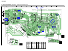
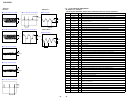
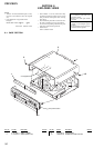
CDP-CE575
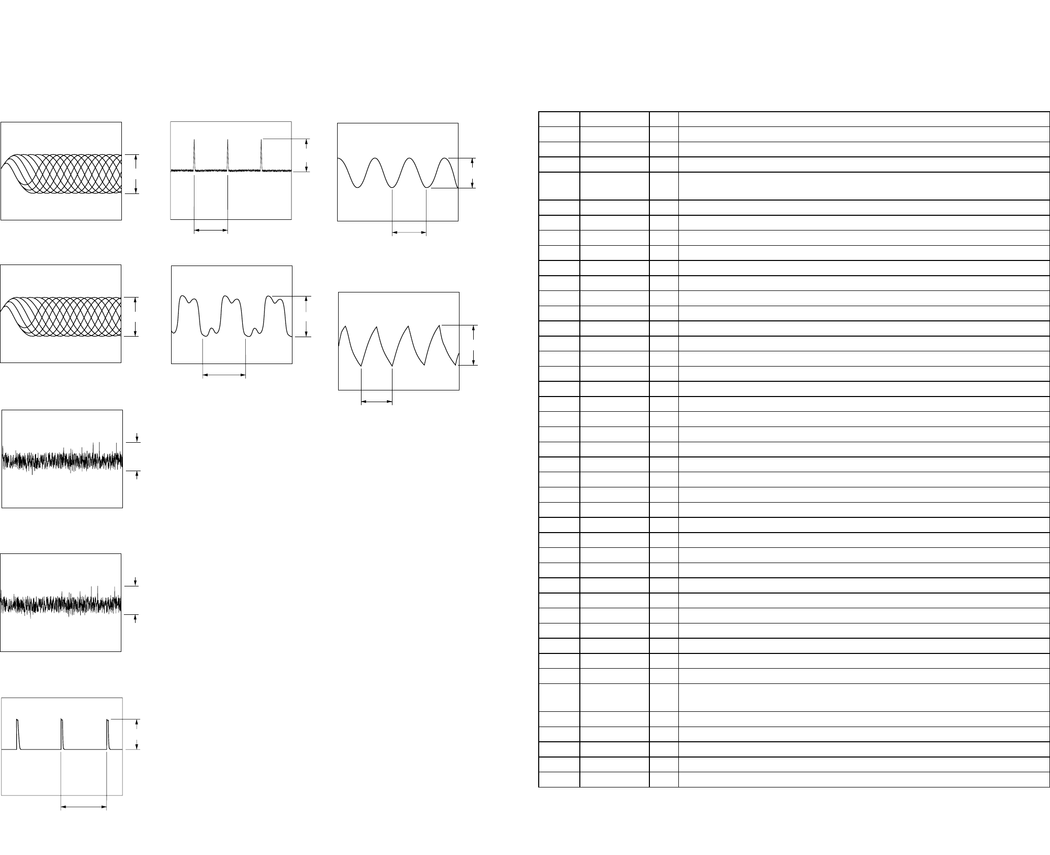
3232
1 IC101 ta (RFAC) (CD Play Mode) 6 IC101 w; (SCOR) (CD Play Mode)
qa IC301 es (XTAL)
2 IC101 rd (RFDC) (CD Play Mode) 7
IC101 yj (XTAO)
(CD Play Mode)
qs IC801 t; (OSCO)
3 IC101 el (FE) (CD Play Mode)
4 IC101 ra (TE) (CD Play Mode)
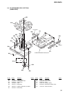
• Waveforms
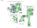
– BD Board –
5 IC101 wh (MDP) (CD Play Mode)
– MAIN Board –
– DISPLAY Board –
1.3 Vp-p
5.2 Vp-p
13.4 ms
5 Vp-p
100 ns
1.4 Vp-p
5.9 Vp-p
59 ns
2.3 Vp-p
508 ns
approx.
200 mVp-p
approx.
400 mVp-p
2.7 V
7.5
µ
s
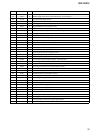
7-11. IC PIN FUNCTION DESCRIPTION
•
Pin No. Pin Name I/O Description
1SQSOO
Subcode Q data output to the system controller (IC301)
2 SQCK I
Subcode Q data reading clock signal input from the system controller (IC301)
3 XRST I
System reset signal input from the system controller (IC301) “L”: reset
4 SYSM I
Analog line muting on/off control signal input terminal “H”: line muting on
Not used (fixed at “L”)
5 DATA I
Command serial data input from the system controller (IC301)
6 XLAT I
Command latch pulse input from the system controller (IC301)
7 CLOK I
Command serial data transfer clock signal input from the system controller (IC301)
8 SENS O
Internal status monitor output to the system controller (IC301)
9 SCLK I
SENSE serial data reading clock input from the system controller (IC301)
10 VDD —
Power supply terminal (+5V) (digital system)
11 ATSK I/O
Input pin for anti-shock Not used (fixed at “L”)
12 SPOA I
Microcomputer escape interface input A terminal Not used (fixed at “L”)
13 SPOB I
Microcomputer escape interface input B terminal Not used (fixed at “L”)
14 XLON O
Microcomputer escape interface output terminal Not used (open)
15 WFCK O
WFCK output terminal Not used (open)
16 XUGF O
Not used (open)
17 XPCK O
Not used (open)
18 GFS O
Not used (open)
19 C2PO O
Not used (open)
20 SCOR O
Subcode sync (S0+S1) detection signal output to the system controller (IC301)
21 COUT I/O
Numbers of track counted signal input/output terminal Not used (open)
22 MIRR I/O
Mirror signal input/output terminal Not used (open)
23 DFCT I/O
Defect signal input/output terminal Not used (open)
24 FOK I/O
Focus OK input/output terminal Not used (open)
25 LOCK I/O
GFS is sampled by 460 Hz “H” when GFS is “H” Not used (open)
26 MDP O
Spindle motor (M101) servo drive signal output to the AN48005B (IC150)
27 SSTP I
Limit in detect switch (S101) input terminal
28 SFDR O
Sled servo drive PWM signal (+) output to the AN48005B (IC150)
29 SRDR O
Sled servo drive PWM signal (–) output to the AN48005B (IC150)
30 TFDR O
Tracking servo drive PWM signal (+) output to the AN48005B (IC150)
31 TRDR O
Tracking servo drive PWM signal (–) output to the AN48005B (IC150)
32 FFDR O
Focus servo drive PWM signal (+) output to the AN48005B (IC150)
33 FRDR O
Focus servo drive PWM signal (–) output to the AN48005B (IC150)
34 VSS —
Ground terminal (digital system)
35 TEST I
Input terminal for the test (fixed at “L”)
36 TES1 I
Input terminal for the test (fixed at “L”)
37 XTSL I
Input terminal for the system clock frequency setting “L”: 45.1584 MHz, “H”: 22.5792 MHz
(fixed at “L” in this set)
38 VC I
Middle point voltage (+2.5V) input from the CXA2581N (IC131)
39 FE I
Focus error signal input from the CXA2581N (IC131)
40 SE I
Sled error signal input from the CXA2581N (IC131)
41 TE I
Tracking error signal input from the CXA2581N (IC131)
42 CE I
Command chip enable signal input from the CXA2581N (IC131)
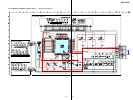
BD BOARD IC101 CXD2587Q
(DIGITAL SIGNAL PROCESSOR, DIGITAL SERVO PROCESSOR, DIGITAL FILTER, D/A CONVERTER)