


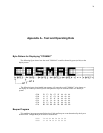
I
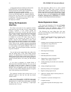
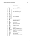
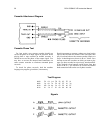
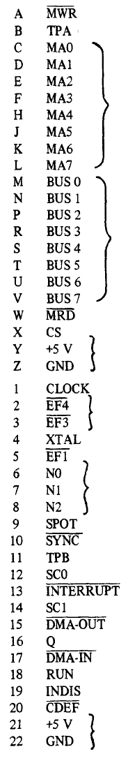
Pin Signal Description
Negative-going memory-write pulse Early
timing pulse for M address clocking, etc.
Memory address lines. High-order address byte
appears on these lines during TPA time.,
followed by low-order address byte
8-bit, 2-way tri-state data bus
Low for memory read machine cycles
Chip select for operating system
Optional power for external logic
CDP1802 clock output
Flag input lines #3 and #4
(Flag 3 also used for hex keyboard)
Crystal frequency
Flag input line #1
Low-order 3 bits of N during
6N instruction
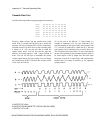
Video spot output
Video sync output
Timing pulse for clocking memory byte out, etc.
State code bit (+5 V for SI /S3, GND for SO/S2)
Pulling to GND causes interrupt (22-KE2 input)
State code bit (+5 V for S2/S3, GND for SO/Sl)
Pull to GND for DMA-OUT cycles
Q flip-flop output line
Pull to GND for DMA-IN cycles
+5 V when running, GND when RUN switch down
Internal RAM-disable input
GND when RAM pages C, D, E, and F selected
Optional power for external logic (same as Y-Z)
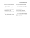
Table III - External Option Terminal Connections
(See Fig. E-2, Appendix E)
V1. Expansion Considerations and Connections .25