


TDA8559_3 © Koninklijke Philips Electronics N.V. 2006. All rights reserved.
Product data sheets Rev. 03 — 15 May 2006 11 of 36
Philips Semiconductors
TDA8559T
Low-voltage stereo headphone amplifier
[1] The supply voltage range at pin V
P1
is from 1.9 V to 18 V. Pin V
P2
is used for the voltage range from 6 V to 30 V.
[2] Measured with low-pass filter 30 kHz.
[3] Noise output voltage measured with a bandwidth of 20 Hz to 20 kHz, unweighted. R
s
=5kΩ.
[4] RMS output voltage in mute is measured with V
i
= 200 mV (RMS); f = 1 kHz.
[5] DC output offset voltage is measured between the signal output and the 0.5V
P
output.
[6] The ripple rejection is measured with a ripple voltage of 200 mV (RMS) applied to the positive supply rail (R
s
=0kΩ).
[7] DC output offset voltage is measured between the two signal outputs.
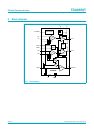
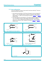
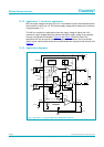
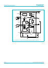
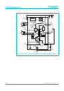
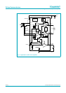
13. Application information
13.1 General
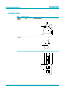
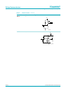
For applications with a maximum supply voltage of 6 V (input mode low) the input pins
need a DC path to ground (see Figure 3 and Figure 4). For applications with supply
voltages in the range from 6 V to 18 V (input mode HIGH) the input DC level is
0.5V
P
+ 0.6 V. In this situation the input configurations illustrated in Figure 5 and Figure 6
have to be used.
V
no
noise output voltage
[3]
-7085µV
V
no(mute)
noise output voltage in
mute
[3]
-2030µV
V
o(mute)
output voltage in mute
[4]
--30µV
V
mt
mid-tap voltage 1.4 1.5 1.6 V
Z
i
input impedance 75 100 125 kΩ
V
os
DC output offset voltage
[5]
- - 100 mV
SVRR supply voltage ripple
rejection
[6]
45 55 - dB
BTL application (R
L
= 25 Ω)
P
o
output power THD = 10 % 125 140 - mW
THD total harmonic distortion P
o
= 70 mW; f
i
= 1 kHz - 0.05 0.1 %
P
o
= 70 mW; f
i
= 10 kHz - 0.1 - %
G
v
voltage gain 31 32 33 dB
f
ss
small signal roll-off
frequency
−1 dB - 750 - kHz
V
no
noise output voltage
[3]
- 100 120 µV
V
no(mute)
noise output voltage in
mute
[3]
-2540µV
V
o(mute)
output voltage in mute
[4]
--40µV
Z
i
input impedance 39 50 61 kΩ
V
os
DC output offset voltage
[7]
- - 150 mV
SVRR supply voltage ripple
rejection
[6]
39 49 - dB
Line driver application (R
L
= 1 kΩ)
V
o
line output voltage 0.1 - 2.9 V
Table 7. Characteristics
…continued
V
P
= 3 V; T
amb
= 25
°
C; f
i
= 1 kHz; unless otherwise specified.
Symbol Parameter Conditions Min Typ Max Unit