


9397 750 13928 © Koninklijke Philips Electronics N.V. 2004. All rights reserved.
Product data Rev. 03 – 23 August 2004 8 of 31
Philips Semiconductors
PNX2000
Audio video input processor
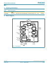
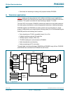
In the tables that follow, signals of the PNX2000 have been sorted by functional group. For
quick reference Ta bl e 4
identifies each functional group and associated table.
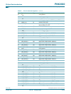
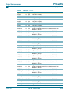
142 V
SSE
- 3.3 V ground
143 V
DDE
- 3.3 V supply voltage
144 V
SSE
- 3.3 V ground
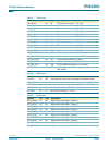
Table 4: Signal groups
Functional group Table number
I
2
D-bus Ta ble 5
AUDIO Ta ble 6
I
2
S-bus Ta ble 7
VIDDEC Ta ble 8
ITU-656 Ta ble 9
JTAG Ta ble 10
I
2
C-bus Ta ble 11
CLOCK Ta ble 12
GTU Ta ble 13
RESET Tabl e 14
DIGITAL SUPPLY Ta ble 15
ANALOG SUPPLY Ta ble 16
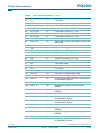
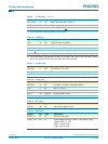
Table 5: I
2
D pins
Symbol Pin Type Description
DLINK1DP 2 IA analog differential data link 1 positive termination
DLINK1DN 3 IA analog differential data link 1 negative termination
DLINK1SP 4 IA analog differential strobe link 1 positive termination
DLINK1SN 5 IA analog differential strobe link 1 negative termination
DLINK2DP 7 IA analog differential data link 2 positive termination
DLINK2DN 8 IA analog differential data link 2 negative termination
DLINK2SP 9 IA analog differential strobe link 2 positive termination
DLINK2SN 10 IA analog differential strobe link 2 negative termination
DLINK3DP 12 IA analog differential data link 3 positive termination
DLINK3DN 13 IA analog differential data link 3 negative termination
DLINK3SP 14 IA analog differential strobe link 3 positive termination
DLINK3SN 15 IA analog differential strobe link 3 negative termination
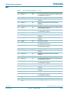
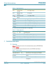
Table 6: Audio pins
Symbol Pin Type Description
ADAC1 104 OA analog audio output 1
ADAC2 107 OA analog audio output 2
ADAC3 110 OA analog audio output 3
ADAC4 113 OA analog audio output 4
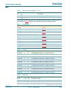
Table 3: Pins in numerical sequence
…continued
Pin Symbol Type Description