


9397 750 13928 © Koninklijke Philips Electronics N.V. 2004. All rights reserved.
Product data Rev. 03 – 23 August 2004 12 of 31
Philips Semiconductors
PNX2000
Audio video input processor
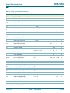
[1] V
DDI
and V
DDM
can be connected to same 1.8 V supply voltage.
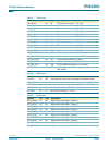
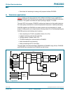
7. Functional description
7.1 Overview
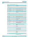
Table 17 describes the functions of the hardware blocks (see also PNX2000 Block
Diagram Figure 1
).
For more detailed functional description refer to the PNX2000 User Manual.
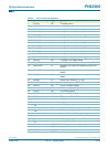
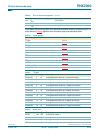
Table 15: Digital supply pins
Symbol Pin Type Description
V
DDE
32,49,66, 82,91,
141,143
- 3.3 V supply voltage
V
SSE
28,41,59, 72,99,
142,144
- 3.3 V ground
V
DDI
[1]
30,35,53,67, 80,97 - 1.8 V supply voltage
V
SS
29,36,43, 54,68,81,
98,139
- 1.8 V ground
V
DDM
[1]
44,140 - 1.8 V supply voltage for KSFRAMs and KROMs
V
SSD(I2D)
1GDI
2
D digital ground
V
DDD(I2D)
16 SD I
2
D digital 1.8 V supply voltage
V
SS(ADAC)
100 GD audio DAC 1.8 V digital ground
V
DDD(ADAC)
101 SD audio DAC 1.8 V digital supply voltage
V
DD3(DTC)
23 SD DTC 3.3 V supply voltage
V
DDD(DTC)
24 SD DTC 1.8 V supply voltage
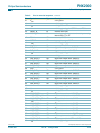
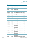
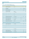
Table 16: Analog supply pins
Symbol Pin Type Description
V
SSA(I2D)
6GA I
2
D analog ground
V
DDA(I2D)
11 SA I
2
D analog 1.8 V supply voltage
V
DDA(PLL)
33 - phase locked loop 1.8 V supply voltage
V
DDA(ADAC)
102 SA audio DAC 3.3 V supply voltage
V
SS(DTC)
25 GA DTC analog ground
V
DDA(XTAL)
37 OSCVDD 1.8 V crystal oscillator supply voltage
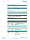
Table 17: Block function
Function Block Description
High speed data link I
2
D Receives data in three streams from PNX3000.
Video decoder
processor
VIDDEC Decodes and processes CVBS, YUV or Y/C in YUV
stream.
Serial interface I
2
C-bus To access all the internal registers.
Global Task Unit GTU Generates all the internal clocks, reset and power
management.