


9397 750 13928 © Koninklijke Philips Electronics N.V. 2004. All rights reserved.
Product data Rev. 03 – 23 August 2004 11 of 31
Philips Semiconductors
PNX2000
Audio video input processor
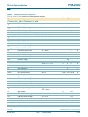
[1] It is recommended to bias this pad with a 10 kΩ resistor
[1] It is recommended to pull-down TRST_N with a 10 kΩ resistor. This ensures correct reset state of internal
TAP circuitry and correct POR of the device within defined state machine.
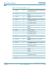
DVO_VALID 52 OD digital video data valid; CMOS; Z
DVO_CLK 51 OD digital video output clock; CMOS; Z
LL_CLK 50 ID reserved; TTL; 5VT
[1]
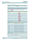
Table 10: JTAG pins
Symbol Pin Type Description
TDO 93 OD JTAG test data out; CMOS
TDI 92 ID JTAG test data in; TTL-H; 5VT
TCK 94 ID JTAG test clock; TTL-H; 5VT
TRST_N
[1]
96 ID JTAG reset (active low); TTL-H; 5VT
TMS 95 ID JTAG test mode select; TTL-H; 5VT
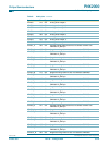
Table 11: I
2
C-bus pins
Symbol Pin Type Description
I2C_SDA 27 IOD I
2
C-bus data; TTL; Z; 5VT
I2C_SCL 26 IOD I
2
C-bus clock; TTL; Z; 5VT
I2C_ADR 17 ID I
2
C-bus address select (internal pull-down); TTL; 5VT
Table 12: Clock pins
Symbol Pin Type Description
MPIFCLK 31 OD 13.5 MHz or 27 MHz to PNX3000; CMOS
DCLK 47 OD reserved; CMOS
XIN 38 OSCIN crystal oscillator input
XOUT 39 OSCOUT crystal oscillator output
XGND 40 OSCGND crystal oscillator ground
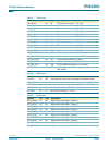
Table 13: GTU pins
Symbol Pin Type Description
INTOUT 48 OD interrupt line output; Z; 5VT
Table 14: Reset pins
Symbol Pin Type Description
RESET_N 45 IA external reset input
RESET_SEL 46 ID selects between using an external reset input or using
internal POR; TTL; 5VT
HIGH = internal reset
LOW = external reset
Table 9: ITU-656 pins
…continued
Symbol Pin Type Description