


2000 Oct 16 6
Philips Semiconductors Product specification
GSM/DCS/PCS power amplifier CGY2014TT
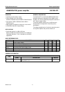
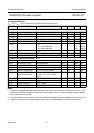
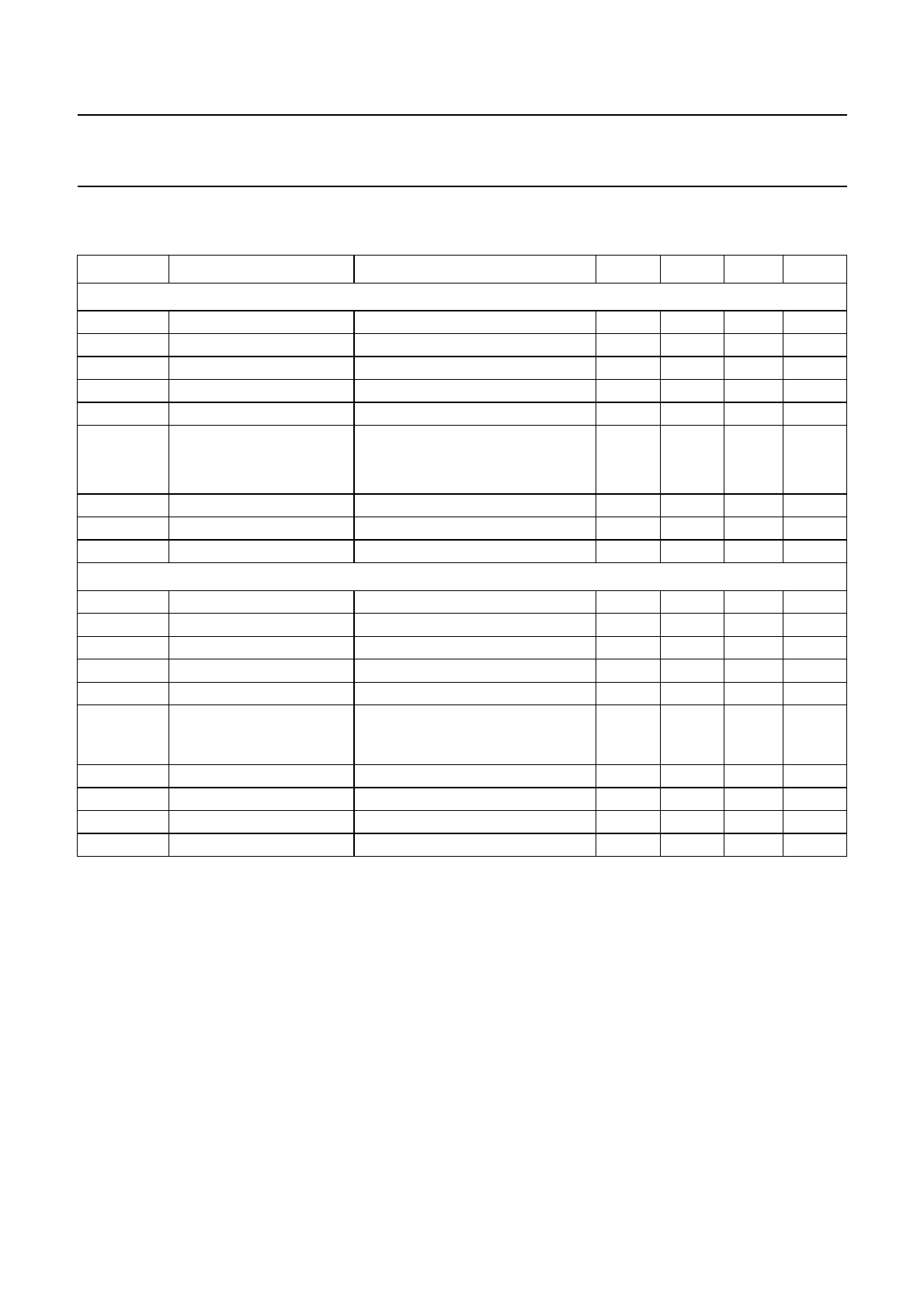
AC CHARACTERISTICS
V
DD
= 3.5 V; T
amb
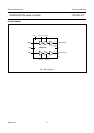
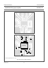
=25°C; measured on the Philips demoboard (see Fig.8).
Notes
1. The device is adjusted to provide nominal load power into a 50 Ω load. The device is switched off and a 6 : 1 load
replaces the 50 Ω load. The device is switched on and the phase of the 6 : 1 load is varied 360 electrical degrees
during a 60 seconds test period.
2. The power amplifier can be matched to PCS and or DCS/PCS operation through optimization of the matching circuit.
3. Isolation can be improved to −20 dBm (typical value) with a pin diode switched in the DCS output matching.
SYMBOL PARAMETER CONDITIONS MIN. TYP. MAX. UNIT
Low band: GSM power amplifier
P
i(LB)
input power −2 0 +2 dBm
f
RF(LB)
RF frequency range 880 − 915 MHz
P
o(LB)(max)
maximum output power see Figs 3 and 4 34.5 35 − dBm
η
LB
efficiency see Fig.3 50 55 − %
P
o(LB)(min)
minimum output power V
DD
=0V; P
i(LB)
= 0 dBm −−35 − dBm
N
RX(LB)
output noise in RX band P
i(LB)
= 0 dBm
f
RF
= 925 to 935 MHz −−−117 dBm/Hz
f
RF
= 935 to 960 MHz −−−129 dBm/Hz
H2
LB
2nd harmonic level P
i(LB)
= 0 dBm −−−35 dBc
H3
LB
3rd harmonic level P
i(LB)
= 0 dBm −−−35 dBc
Stab
LB
stability P
i(LB)
= 0 dBm; note 1 −−−60 dBc
High band: DCS/PCS power amplifier; note 2
P
i(HB)
input power 2 3 5 dBm
f
RF(HB)
RF frequency range for DCS operation 1710 − 1785 MHz
P
o(HB)(max)
maximum output power see Figs 5 and 6 32 32.5 − dBm
η
HB
efficiency see Fig.5 38 40 − %
P
o(HB)(min)
minimum output power V
DD
=0V; P
i(HB)
= 3 dBm −−32 − dBm
α
HB
high band isolation when
low band is operating
V
DD(LB)
= 3.5 V; P
i(LB)
= 0 dBm;
V
DD(HB)
=0V; P
i(HB)
= 3 dBm;
note 3
− 0 − dBm
N
RX(HB)
output noise in RX band P
i(HB)
= 3 dBm −−−121 dBm/Hz
H2
HB
2nd harmonic level P
i(HB)
= 3 dBm −−−35 dBc
H3
HB
3rd harmonic level P
i(HB)
= 3 dBm −−−35 dBc
Stab
HB
stability P
i(HB)
= 3 dBm; note 1 −−−60 dBc