


2000 Oct 16 5
Philips Semiconductors Product specification
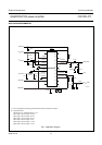
GSM/DCS/PCS power amplifier CGY2014TT
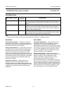
LIMITING VALUES
In accordance with the Absolute Maximum Rating System (IEC 60134).
Note
1. The total power dissipation is measured under GSM pulse conditions in a good thermal environment;
see
“Application Note CTT0003”
.
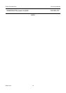
THERMAL CHARACTERISTICS
Note
1. This thermal resistance is measured under GSM pulse conditions in a good thermal environment;
see
“Application Note CTT0003”
.
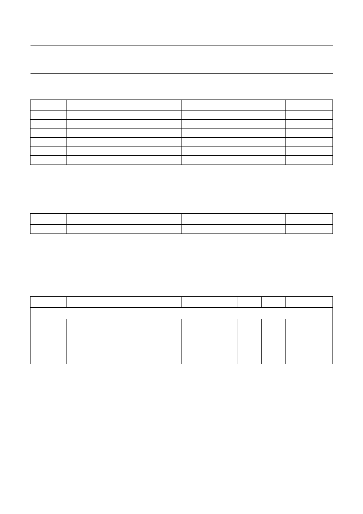
DC CHARACTERISTICS
V
DD
= 3.5 V; T
amb
=25°C; general operating conditions applied; peak current values measured during burst; unless
otherwise specified.
Notes
1. The supply circuit includes a (drain) MOS switch with R
DSon
=40mΩ. The battery voltage is 3.6 V (typical value).
2. No RF input signal or P
i(LB)
< −30 dBm; V
DD
=1V.
3. No RF input signal or P
i(HB)
< −30 dBm; V
DD
=1V.
SYMBOL PARAMETER CONDITIONS MAX. UNIT
V
DD
positive supply voltage 5.2 V
T
j(max)
maximum operating junction temperature 150 °C
T
stg
storage temperature 150 °C
P
tot
total power dissipation note 1 2.0 W
P
i(LB)
GSM input power 10 dBm
P
i(HB)
DCS/PCS input power 10 dBm
SYMBOL PARAMETER CONDITIONS VALUE UNIT
R
th(j-c)
thermal resistance from junction to case note 1 30 K/W
SYMBOL PARAMETER CONDITIONS MIN. TYP. MAX. UNIT
Supplies: pins V
DD1LB
, V
DD2LB
, RFO/V
DD3LB
, V
DD1HB
, V
DD2HB
and RFO/V
DD3HB
V
DD
positive supply voltage note 1 0 3.5 4.2 V
I
DD(LB)
GSM positive peak supply current P
i(LB)
= 0 dBm − 2 − A
note 2 0.5 1.5 3 A
I
DD(HB)
DCS/PCS positive peak supply current P
i(HB)
= 3 dBm − 1.5 − A
note 3 0.25 1 2 A