


2000 Oct 16 4
Philips Semiconductors Product specification
GSM/DCS/PCS power amplifier CGY2014TT
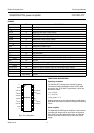
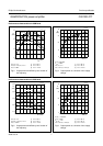
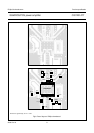
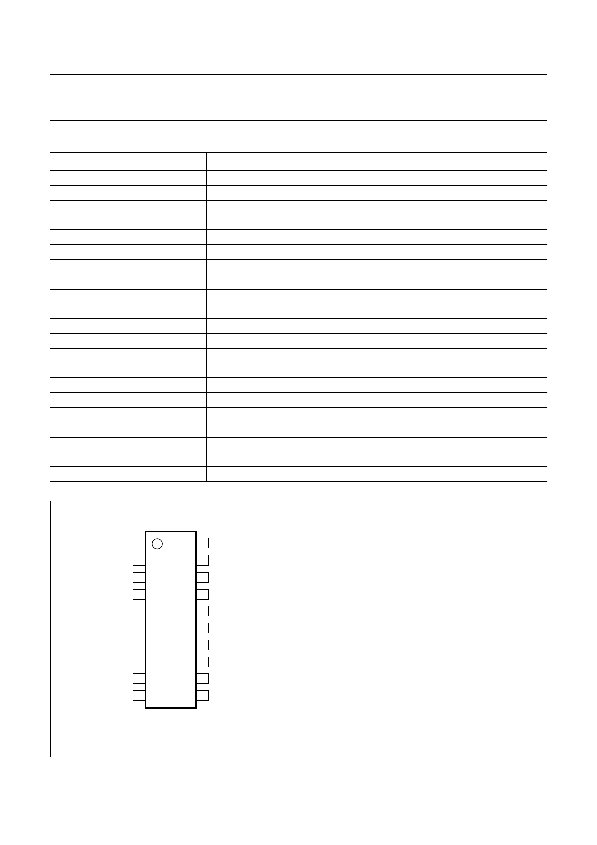
PINNING
SYMBOL PIN DESCRIPTION
n.c. 1 not connected
RFI
HB
2 DCS/PCS power amplifier input
V
DD1HB
3 DCS/PCS first stage supply voltage
V
DD2HB
4 DCS/PCS second stage supply voltage
V
DD2HB
5 DCS/PCS second stage supply voltage
V
DD2LB
6 GSM second stage supply voltage
V
DD1LB
7 GSM first stage supply voltage
GND1
LB
8 GSM first stage ground
RFI
LB
9 GSM power amplifier input
n.c. 10 not connected
n.c. 11 not connected
n.c. 12 not connected
RFO/V
DD3LB
13 GSM power amplifier output and third stage supply voltage
RFO/V
DD3LB
14 GSM power amplifier output and third stage supply voltage
GND 15 ground
n.c. 16 internal connection to ground; pin should not be connected to the board
RFO/V
DD3HB
17 DCS/PCS power amplifier output and third stage supply voltage
RFO/V
DD3HB
18 DCS/PCS power amplifier output and third stage supply voltage
n.c. 19 not connected
n.c. 20 not connected
− exposed die ground
FUNCTIONAL DESCRIPTION
Operating conditions
The CGY2014TT is designed to meet the European
Telecommunications Standards Institute (ETSI) GSM
documents, the
“ETS 300 577 specification”
, which are
defined as follows:
• t
on
= 570 µs
• T = 4.16 ms
• Duty cycle δ =
1
/
8
.
Multislot operation can be implemented provided that the
application circuit does not drive the IC beyond the limiting
values.
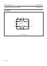
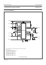
Power amplifier
The GSM and DCS/PCS power amplifiers consist of three
cascaded gain stages with an open-drain configuration.
Each drain has to be loaded externally by an adequate
reactive circuit which also has to be a DC path to the
supply.
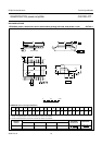
handbook, halfpage
CGY2014TT
FCA181
1
2
3
4
5
6
7
8
9
10
n.c.
RFI
HB
V
DD1HB
V
DD2HB
V
DD2HB
V
DD2LB
V
DD1LB
GND1
LB
RFI
LB
n.c.
n.c.
n.c.
RFO/V
DD3HB
RFO/V
DD3HB
n.c.
GND
RFO/V
DD3LB
RFO/V
DD3LB
n.c.
n.c.
20
19
18
17
16
15
14
13
12
11
Fig.2 Pin configuration.