


4-1
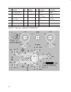
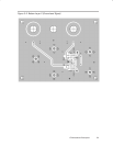
High-Speed Amplifier PCB Layout Tips
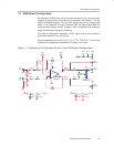
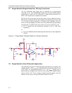
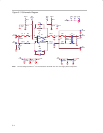
The THS4503EVM layout has been designed for use with high-speed signals
and can be used as an example when designing PCBs incorporating the
THS4503. Careful attention has been given to component selection,
grounding, power supply bypassing, and signal path layout. Disregarding
these basic design considerations could result in less than optimum
performance of the THS4503 high-speed operational amplifier. Surface-
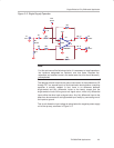
mount components were selected because of the extremely low lead
inductance associated with this technology. This helps minimize both stray
inductance and capacitance. Also, because surface-mount components are
physically small, the layout can be very compact.
Tantalum power supply bypass capacitors at the power input pads help filter
switching transients from the laboratory power supply. Power supply bypass
capacitors are placed as close as possible to the IC power input pins in order
to minimize the return path impedance. This improves high frequency
bypassing and reduces harmonic distortion. The GND side of these capacitors
should be located close to each other, minimizing the differential current loops
associated with differential output currents. If poor high frequency
performance is observed, replace the 0.1-µF capacitors with microwave
capacitors with a self-resonance at the frequency that produces trouble. A
proper ground plane on both sides of the PCB should be used with high-speed
circuit design. This provides low-inductive ground connections for return
current paths.
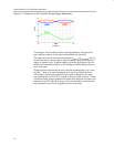
In the area of the amplifier input pins, however, the ground plane has been
removed to minimize stray capacitance and reduce ground plane noise
coupling into these pins. This is especially important for the inverting input pin.
As low as 1 pF capacitance at the inverting input can significantly affect the
response of the amplifier or even oscillation.
In general, it is best to keep signal lines as short and as straight as possible.
Incorporation of microstrip or stripline techniques is also recommended when
signal lines are greater than 1 inch in length. These traces must be designed
with a characteristic impedance of either 50 Ω or 75 Ω, as required by the
application. Such a signal line must also be properly terminated with an
appropriate resistor.
Chapter 4