


Description
1-2
1.1 Description
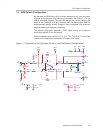
The THS4503EVM provides a platform for developing high-speed FDA
application circuits. It contains the THS4503 high-speed FDA, a number of
passive components, and various features and footprints that enable the user
to experiment, test, and verify various operational amplifier circuit
implementations. The PC board measures 3.08 by 2.42 inches.
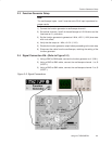
1.2 Evaluation Module Features
THS4503 high-speed operational amplifier EVM features include:
- Wide operating supply voltage range: single supply 5 Vdc to dual supply
±5 Vdc operation (see the device data sheet). Single supply operation is
obtained by placing a jumper from GND (J7) to –V
S
(J5).
- Single-ended and fully differential input capability
- Single-ended and fully differential output capability
- Nominal 50-Ω input termination (R1||R2). Termination can be configured
according to the application requirement.
- V
OCM
direct input through TP1
- Output transformer T1
- Footprints for antialiasing filter implementation using locations R6, R7, C5,
and C6
- Footprints for low pass filter implementation using locations C3, C4
- 800-Ω load provided through R8, R10, R9, and R11 reflected through T1
- Three convenient GND test points on the PCB
- Power supply ripple rejection capacitors (C8 and C11)
- Decoupling capacitors (C9, C12) populated with 0.1 µF capacitors—
design final decoupling in accordance with SLOA069.
- PowerPAD heatsinking capability
- A good example of high-speed amplifier PCB design and layout
1.3 THS4503EVM Operating Conditions
- Supply voltage range, ±V
S
5 V to ±5 V (see the device data sheet)
- Supply current, I
S
(see the device data sheet)
For complete THS4503 amplifier IC specifications, parameter measurement
information, and additional application information, see the THS4503 data
sheet, TI literature number SLOS350.