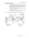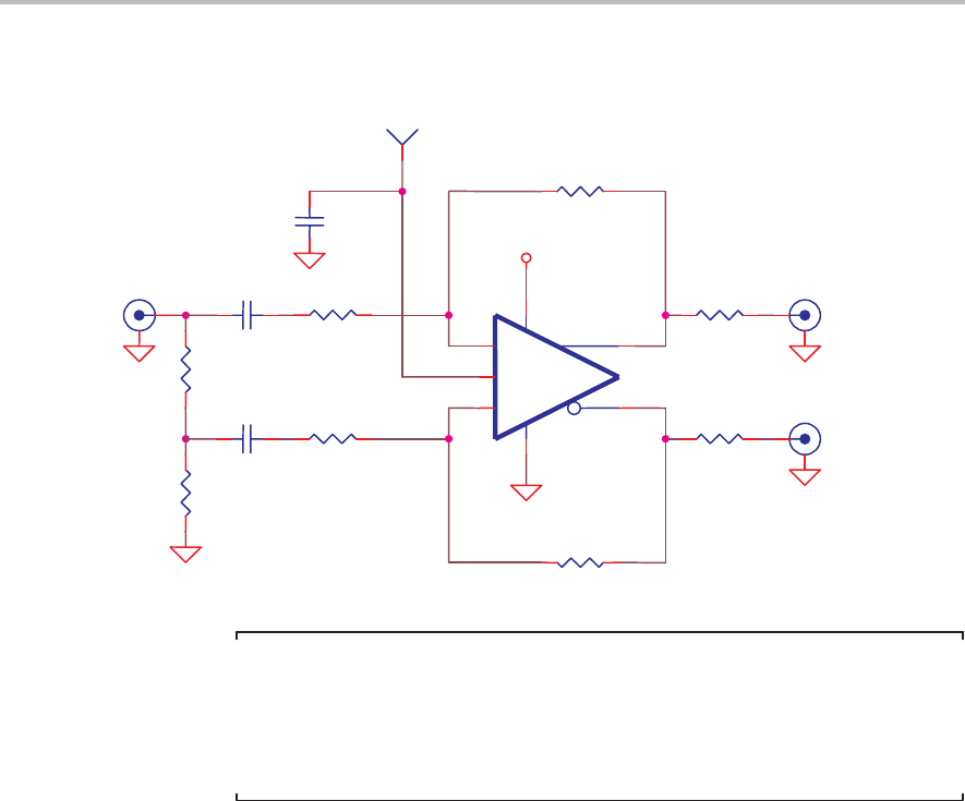
Single-Ended to Fully Differential Application
3-3
THS4503EVM Applications
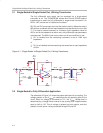
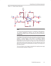
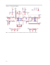
Figure 3−2. Single Supply Operation
TP1
Vocm
R1
56.2
W
J3
Vout−
R5
392
W
J2
Vout+
J1
Vin−
C2
R3
402
W
R4
392
W
+VS
−
Vocm
+
U1
THS4503
1
8
2
3
6
5
4
C1
R17
0
R7 0
R6 0
C13
1
m
F
R2
374
W
Note:
For this and some of the following circuits, it is necessary to install capacitors
into locations designated as resistors, and vice versa. Because the
capacitors and resistors come in the same case size, this should be easily
accomplished.
The designer should note that the ground connection of the schematic at C2
through R17 is a second input—to avoid confusion about whether a coupling
capacitor is actually needed. In fact, there is no difference between
single-ended and fully differential inputs to the board, except that the
single-ended circuits utilize ground as signal return, while fully differential
inputs utilize the other input as signal return. Any fully differential input to the
board can be converted to a single-ended input merely by connecting one of
the inputs to ground.
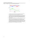
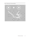
This circuit allows the input voltage to swing below the negative power supply
rail of the op-amp, as shown in Figure 3−3.


