


PSU Interface (J150)
2-2
2.1 PSU Interface (J150)
The TAS5110D6DAD board must be powered from external power supplies.
High-end audio performance requires a stabilized power supply with low ripple
voltage and low output impedance.
Note:
The length of the power-supply cable must be minimized. Increasing the
impedance of the PSU cable is equal to increasing the distortion for the
amplifier at high output levels and low frequencies.
The maximum output stage supply voltage depends on the speaker load
resistance. See the recommended maximum supply voltage in Chapter 4.
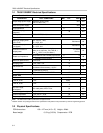
Description R
L
= 4 Ω R
L
= 6 Ω R
L
= 8 Ω
Supply voltage for output stage 0 V – 20 V 0 V – 26.5 V 0 V – 26.5 V
Supply voltage for gate drive 22 V (min 16.5 V, max 26.5 V)
Supply voltage for control 5 V (min 4.5 V, max 5.3 V)
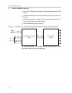
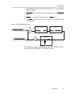
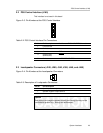
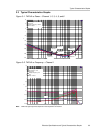
The recommended TAS5110 power-up sequence is shown in Figure 2–1. For
proper TAS5110 operation, the RESET signal should be kept low during power
up. RESET
is pulled low during power up for 100 ms by the onboard low-drop
linear regulator (U170).
Figure 2–1. Recommended TAS5110 Power-Up Sequence
Output Stage Supply
RESET
Gate-Drive Supply
Control Supply (3.3 V)
>1 ms
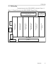
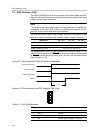
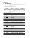
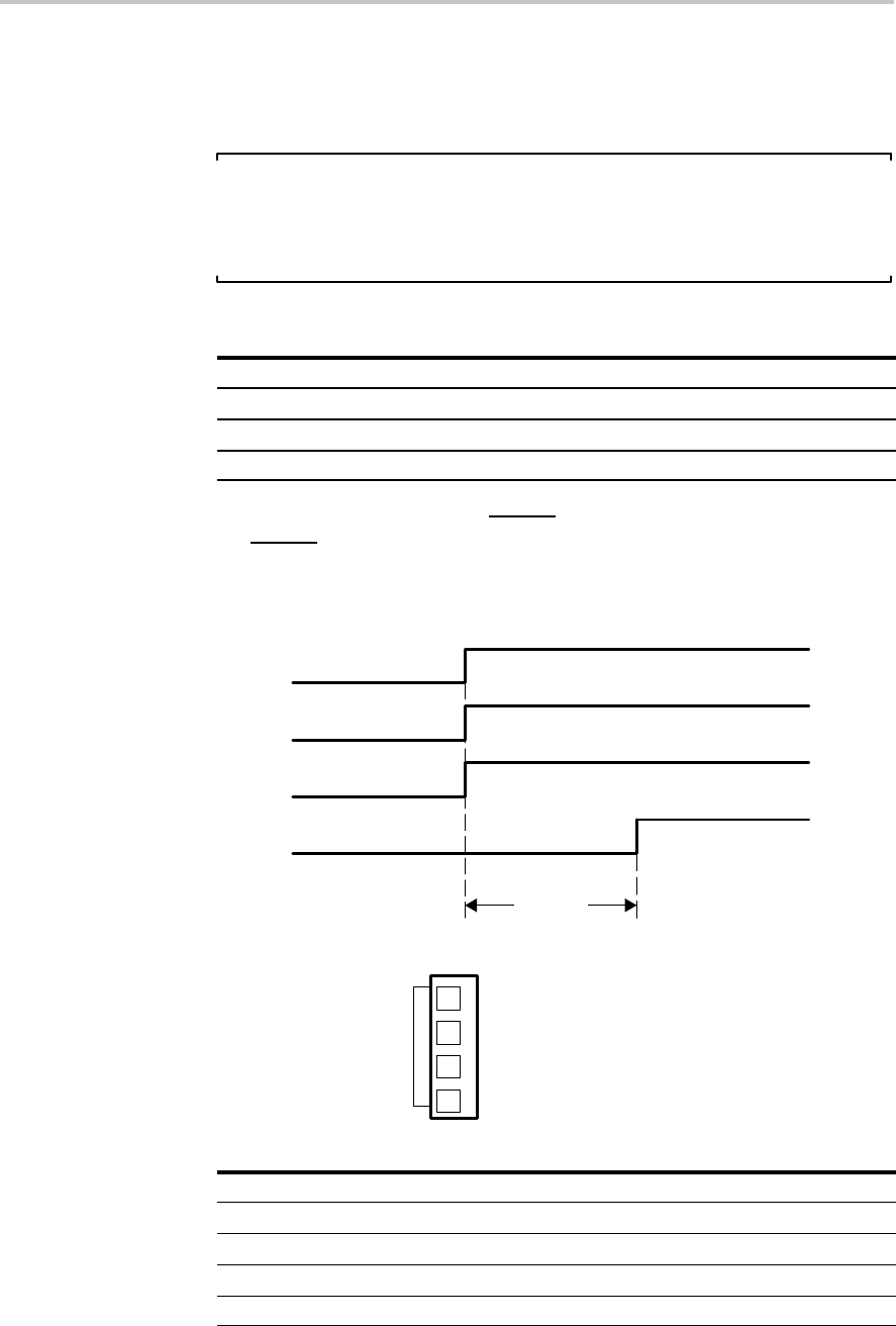
Figure 2–2. Pin Numbers at the PSU Interface (Top View)
4
1
2
3
Table 2–1.J150 Pin Description
Pin No. Net Name at Schematic Description
1 Power output stage H-bridge supply voltage
2 GND Ground
3 Gate-drive supply Gate-drive supply voltage (I ≈ 90 mA)
4 5 V Control supply voltage (I ≈ 100 mA)