


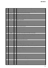
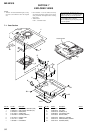

55
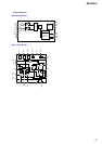
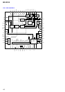
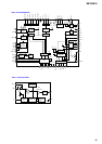
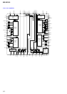
MZ-NF610
Pin No.
166
167
168
169
170
171
172
173
174
175
176
177
178
179
180
181
182
183
184
185
186
187
188
189
190
191
192
193
194
195, 196
197
198
199
200
201
202 to 204
205, 206
207
208
209
210
211
212
213
214, 215
216 to 231
232 to 245
246
247
248
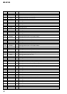
I/O
I
I
I
I
I
I
I
I
I/O
I/O
I/O
O
O
I
O
I
O
I/O
I
O
I/O
O
O
O
I
I
I
I
I
O
I
O
O
O
O
O
O
I
I
I
I
O
I
I
I
—
—
—
—
—
Pin Name
WK_DET
BATT_MON
HALF_LOCK_SW
RMC_KEY
JOG_PUSH
REC_KEY/PLAY_KEY
END_SEARCH
RADIO_ON
RMC_DTCK
UDP
UDM
SUSPEND
UPUEN
UOSCI
UOSCO
SI3
SO3
SCK3
MSIN
MSOUT
MSCK
RF_PWR
LCD_PWR
SP_AMP
XHP_DET
SET_CODE0
SET_CODE1
SET_CODE2
SET_CODE3
NC
VBUS5V_DET
LG_DCR_CTL
MUTE
CLV_PWR_SEL
CS_RTC
MODE1 to 3
HD_CON_1, 2
TAT
TAN
NAR
IOD
SAK
XRST
TRST
TEST0, 1
D0 to 15
A00 to 13
XCAS
XRAS
XWE
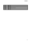
Description
Set key WAKE detection signal input
External battery voltage monitor input Not used (connected to the ground)
Open button detection switch input (A/D input) “L” : the open button is pressed
Key input (A/D input) from the remote commander
Jog dial push detection signal input Not used (open)
REC key input (A/D input)
END SEARCH key input (A/D input) Not used (open)
RADIO ON detection signal input
TSB master data clock input/output or SSB data input/output
USB data (+) input terminal
USB data (-) input terminal
USB suspend signal output Not used (open)
USB pull-up resistor connection control output terminal
Resonator (48MHz) connection terminal for the USB oscillation circuit
Resonator (48MHz) connection terminal for the USB oscillation circuit
Not used (connected to the ground)
Not used (open)
Not used (open)
Not used (connected to the ground)
Not used (open)
Not used (open)
Power supply control signal output to the RF amplifier Not used (open)
Power supply control signal output to the liquid crystal display module Not used (open)
Built-in speaker control signal output “H”: activate Not used (open)
Headphone jack detection signal input Not used (open)
Input terminal for the set (open in this set)
Input terminal for the set (open in this set)
Input terminal for the set (open in this set)
Input terminal for the set (fixed at “L” in this set)
Not used (open)
USB power supply voltage detection terminal 2 Not used (open)
LG DCR control signal output Not used (open)
Analog muting control signal output to the headphone amplifier “H”: muting ON
CLV motor power supply selection control signal output Not used (open)
Chip select signal output to the real time clock Not used (open)
Power supply control signal output for the over write head to the REC driver
Over write head control signal output to the REC driver
Not used (open)
Not used (open)
Not used (open)
Not used (open)
Not used (open)
System reset signal input from the power control “L”: reset
Terminal for the test mode setting (normally fixed at “L”)
Input terminal for the main test (normally fixed at “L”)
DRAM data0 to 15 terminal Not used (open)
DRAM address0 to 13 terminal Not used (open)
DRAM CAS terminal Not used (open)
DRAM RAS terminal Not used (open)
DRAM write enable terminal Not used (open)