


MDX-C5960R/C5970/C5970R
– 29 –
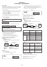
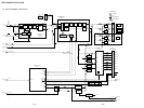
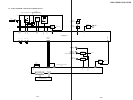
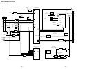
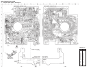
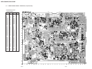
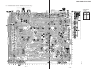
4-6. NOTES FOR PRINTED WIRING BOARDS AND SCHEMATIC DIAGRAMS
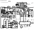
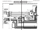
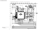
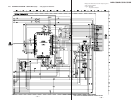
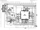
Note on Schematic Diagram:
• All capacitors are in µF unless otherwise noted. pF: µµF
50 WV or less are not indicated except for electrolytics
and tantalums.
• All resistors are in Ω and
1
/
4
W or less unless otherwise
specified.
•
¢
: internal component.
• C : panel designation.
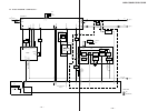
Note on Printed Wiring Board:
• X : parts extracted from the component side.
• Y : parts extracted from the conductor side.
•
r
: Through hole.
•
¢
: internal component.
• b : Pattern from the side which enables seeing.
(The other layers' patterns are not indicated.)
Note:
The components identi-
fied by mark ! or dotted
line with mark ! are criti-
cal for safety.
Replace only with part
number specified.
Note:
Les composants identifiés par
une marque ! sont critiques
pour la sécurité.
Ne les remplacer que par une
piéce portant le numéro
spécifié.
Caution:
Pattern face side: Parts on the pattern face side seen from
(Conductor Side) the pattern face are indicated.
Parts face side: Parts on the parts face side seen from
(Component Side) the parts face are indicated.
• U : B+ Line.
• H : adjustment for repair.
• Power voltage is dc 14.4V and fed with regulated dc power supply
from ACC and BATT cords.
• Voltages are taken with a VOM (Input impedance 10 MΩ).
Voltage variations may be noted due to normal production toler-
ances.
• Waveforms are taken with a oscilloscope.
Voltage variations may be noted due to normal production toler-
ances.
• Circled numbers refer to waveforms.
• Signal path.
F : FM
f : AM (MW/LW)
L : BUS AUDIO IN
E : MD PLAY
• Abbreviation
CND : Canadian model.
G : German model.