


TDA8950_1 © NXP B.V. 2008. All rights reserved.
Preliminary data sheet Rev. 01 — 9 September 2008 18 of 39
NXP Semiconductors
TDA8950
2 × 150 W class-D power amplifier
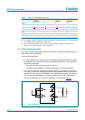
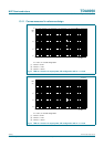
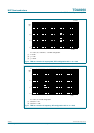
13.3.2 Bridge-Tied Load (BTL)
Maximum output power:
(3)
Maximum current internally limited to 9.2 A:
(4)
Variables:
• R
L
: load impedance
• R
sL
: series impedance of the filter coil
• R
DSon(hs)
: high-side R
DSon
of power stage output DMOS (temperature dependent)
• R
DSon(ls)
: low-side R
DSson
of power stage output DMOS (temperature. dependent)
• f
osc
: oscillator frequency
• t
min
: minimum pulse width (typical 150 ns, temp. dependent)
• V
P
: single-sided supply voltage (or 0.5 × (V
DD
+ |V
SS
|))
• P
o(0.5 %)
: output power at the onset of clipping
Note that I
o(peak)M
should be below 9.2 A (Section 8.3.2). I
o(peak)
is the sum of the current
through the load and the ripple current. The value of the ripple current is dependent on the
coil inductance and voltage drop over the coil.
13.4 External clock
For duty cycle independent operation of the device, the external clock input frequency is
internally divided by two. This implies that the frequency of the external clock is as twice
as high as the internal clock (typical 2 × 345 kHz = 690 kHz).
If two or more class-D amplifiers are used it is recommended that all devices run at the
same switching frequency. This can be realized by connecting all OCS pins together and
feeding them from an external oscillator. When applying an external oscillator, it is
necessary to force pin OSC to a DC level above SGND. The internal oscillator is disabled
and the PWM modulator will switch with half the externally applied frequency.
The internal oscillator requires an external resistor R
ext(OSC)
and capacitor C
OSC
between
pin OSC and PIN VSSA.
The noise contribution of the internal oscillator is supply voltage dependent. An external
low noise oscillator is recommended for low noise applications running at high supply
voltage.
P
o 0.5%()
R
L
R
L
R
DSon hs()
R
dson ls()
++
------------------------------------------------------------------
2V
P
1t
min
0.5 f
osc
×–()××
2
2R
L
--------------------------------------------------------------------------------------------------------------------------------------------------
=
I
opeak()
2V
P
1t
min
0.5 f
osc
×–()×
R
L
R
DSon hs()
R
DSon ls()
+()2R
sL
++
-------------------------------------------------------------------------------------------
=