


TDA8950_1 © NXP B.V. 2008. All rights reserved.
Preliminary data sheet Rev. 01 — 9 September 2008 13 of 39
NXP Semiconductors
TDA8950
2 × 150 W class-D power amplifier
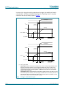
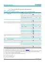
11. Static characteristics
[1] The circuit is DC adjusted at V
P
= ±12.5 V to ±42.5 V.
[2] With respect to SGND (0 V).
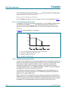
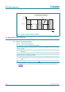
[3] The transition between Standby and Mute mode has hysteresis, while the slope of the transition between Mute and Operating mode is
determined by the time-constant of the RC-network on pin MODE; see Figure 8.
[4] DC output offset voltage is gradually applied to the output during the transition between the Mute and Operating modes. The slope
caused by any DC output offset is determined by the time-constant of the RC-network on pin MODE.
[5] At a junction temperature of approximately T
act(th_fold)
− 5 °C the gain reduction will commence and at a junction temperature of
approximately T
act(th_prot)
the amplifier switches off.
Table 7. Static characteristics
V
P
=
±
35 V; f
osc
= 345 kHz; T
amb
= 25
°
C; unless otherwise specified.
Symbol Parameter Conditions Min Typ Max Unit
Supply
V
P
supply voltage
[1]
±12.5 ±35 ±40 V
V
P(ovp)
overvoltage protection supply voltage non-operating; V
DD
− V
SS
85 - 90 V
V
P(uvp)
undervoltage protection supply voltage V
DD
− V
SS
20 - 25 V
I
q(tot)
total quiescent current Operating mode; no load; no
filter; no RC-snubber network
connected
- 5075mA
I
stb
standby current - 480 600 µA
Mode select input; pin MODE
V
MODE
voltage on pin MODE referenced to SGND
[2]
0 - 6.0 V
Standby mode
[2][3]
0 - 0.8 V
Mute mode
[2][3]
2.2 - 3.0 V
Operating mode
[2][3]
4.2 - 6.0 V
I
I
input current V
I
= 5.5 V - 110 150 µA
Audio inputs; pins IN1M, IN1P, IN2P and IN2M
V
I
input voltage DC input
[2]
-0-V
Amplifier outputs; pins OUT1 and OUT2
V
O(offset)
output offset voltage SE; mute - - ±15 mV
SE; operating
[4]
--±150 mV
BTL; mute - - ±21 mV
BTL; operating
[4]
--±210 mV
Stabilizer output; pin STABI
V
O(STABI)
output voltage on pin STABI mute and operating; with
respect to VSSP1
9.3 9.8 10.3 V
Temperature protection
T
act(th_prot)
thermal protection activation
temperature
- 154 - °C
T
act(th_fold)
thermal foldback activation
temperature
closed loop SE voltage gain
reduced with 6 dB
[5]
- 153 - °C