


TDA8950_1 © NXP B.V. 2008. All rights reserved.
Preliminary data sheet Rev. 01 — 9 September 2008 16 of 39
NXP Semiconductors
TDA8950
2 × 150 W class-D power amplifier
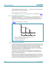
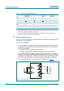
12.3 Mono BTL application characteristics
[1] R
sL
is the series resistance of inductor of low-pass LC filter in the application.
[2] Output power is measured indirectly; based on R
DSon
measurement. See also Section 13.3.
[3] Total harmonic distortion is measured in a bandwidth of 22 Hz to 20 kHz, using an AES17 20 kHz brickwall
filter. Maximum limit is guaranteed but may not be 100 % tested.
[4] V
ripple
= V
ripple(max)
= 2 V (p-p); R
s
= 0 Ω.
[5] B = 22 Hz to 20 kHz, using an AES17 20 kHz brickwall filter. Low noise due to BD modulation.
[6] B = 22 Hz to 20 kHz, using an AES17 20 kHz brickwall filter; independent of R
s
.
[7] V
i
= V
i(max)
= 1 V (RMS); f
i
= 1 kHz.
Table 10. Dynamic characteristics
V
P
=
±
35 V; R
L
= 8
Ω
; f
i
= 1 kHz; f
osc
= 345 kHz; R
sL
< 0.1
Ω
[1]
; T
amb
= 25
°
C; unless otherwise
specified.
Symbol Parameter Conditions Min Typ Max Unit
P
o
output power L = 22 µH; C = 680 nF;
T
j
=85°C; R
L
=8Ω
[2]
THD = 10 %; V
P
= ±39 V - 340 - W
THD = 10 %; V
P
= ±37 V - 300 - W
THD = 0.5 %; V
P
= ±37 V - 200 - W
THD total harmonic
distortion
P
o
= 1 W; f
i
= 1 kHz
[3]
- 0.05 - %
P
o
= 1 W; f
i
= 6 kHz
[3]
- 0.05 - %
G
v(cl)
closed-loop voltage
gain
-36-dB
SVRR supply voltage ripple
rejection
between pin VDDPn and
SGND
operating; f
i
= 100 Hz
[4]
-80-dB
operating; f
i
= 1 kHz
[4]
-80-dB
mute; f
i
= 100 Hz
[4]
-95-dB
standby; f
i
= 100 Hz
[4]
- 120 - dB
between pin VSSPn and
SGND
operating; f
i
= 100 Hz
[4]
-75-dB
operating; f
i
= 1 kHz
[4]
-75-dB
mute; f
i
= 100 Hz
[4]
-90-dB
standby; f
i
= 100 Hz
[4]
- 130 - dB
Z
i
input impedance measured between the input
pins and SGND
45 63 - kΩ
V
n(o)
output noise voltage operating; R
s
=0Ω
[5]
- 190 - µV
mute
[6]
-45-µV
α
mute
mute attenuation f
i
= 1 kHz; V
i
= 2 V (RMS)
[7]
-82-dB
CMRR common mode
rejection ratio
V
i(CM)
= 1 V (RMS) - 75 - dB