


Philips Semiconductors Product data
SA2411+20 dBm single chip linear amplifier for WLAN
2003 Feb 07
4
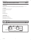
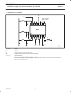
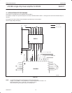
6. FUNCTIONAL DESCRIPTION
The main building-blocks are:
• Fixed gain amplifier (PA)
• Output matching
• Input matching
• Power Detector
• Power Mode
Input
The device has differential inputs so a balun is needed in the case of single ended operation, input impedance is approximately 75 Ω + 25j Ω,
balanced. The inputs can be DC biased with the pin V
DD
_DRIVER. The input matching is optimized to interface with the SA2400A WLAN
transceiver chip.
Amplifier
The amplifier is a fixed gain, class AB amplifier. There is an additional pin, V
DD
_BIAS, to adjust the class A bias current. Reducing the class A
currents reduces the gain. This allows trade-offs to be made among gain, linearity and current.
Output matching
The output of the amplifier is matched, on chip, for a 50 Ω load. The matching includes the supply feed for the power amplifier. The pin
V
DD
_MAIN is the main supply for the amplifier. No additional filtering is needed to meet the 802.11b spec.
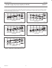
Power detector
The power detector detects the power level and transforms it into a low frequency current. The detector output must be loaded with a resistor to
ground for the highest accuracy. This resistor has an optimal value of 5.6 kΩ. Lower values can be used to comply with maximum input
sensitivity of ADCs, at the cost of dynamic range. The maximum voltage detected is 2.3 V.
Power mode
This pin selects the desired gain and linearity level (13 dB or 14.5 dB gain). The low gain is more applicable to high voltage applications from
3.3 V to 3.6 V. The high gain is more applicable to low voltage applications lower than 3.3 V.
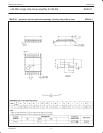
NOTE:
In order to assure optimal thermal performance, it is recommended that all ground pins be connected, and that the number of vias to ground
under the chip be maximized. In addition, the use of solder mask under the chip (for scratch protection) is not recommended.