


Philips Semiconductors Product data
SA2411+20 dBm single chip linear amplifier for WLAN
2003 Feb 07
3
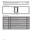
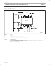
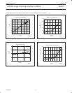
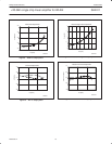
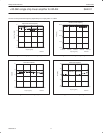
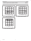
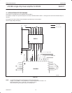
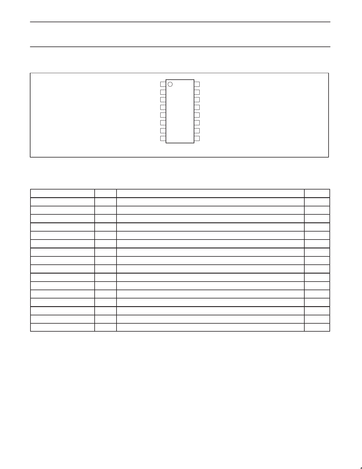
5. PINNING INFORMATION
SR02384
1
2
3
4
5
6
7
89
10
11
12
13
14
15
16V
DD
_MAIN
V
DD
_DRIVER
GND
IN+
IN–
GND
DETECTOR
GND
V
DD
_BIAS
PWRUP
GND
RF_GND
ANT
GND
MODE
GND
SA2411DH
Figure 2. Pin configuration
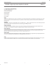
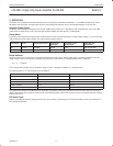
Table 2. Pin description
PIN type is designated by A = Analog, D = Digital, I = Input, O = Output
SYMBOL
PIN DESCRIPTION TYPE
V
DD
_MAIN 1 Analog supply, V
DD
for power amplifier, 150 mA A
V
DD
_DRIVER 2 Analog supply, V
DD
for biasing driver, 35 mA A
GND 3 Grounding A
IN+ 4 Input pin, positive part of balanced signal AI
IN– 5 Input pin, negative part of balanced signal AI
GND 6 Grounding A
DETECTOR 7 Power detector output AO
GND 8 Grounding A
GND 9 Grounding A
MODE 10 Mode switch; floating = high gain, grounded = low gain AI
GND 11 Grounding A
ANT 12 Output pin, RF, to antenna AO
RF_GND 13 RF ground must be connected A
GND 14 Grounding A
PWRUP 15 Power up pin. HIGH = amplifier is on. LOW = amplifier is off. DI
V
DD
_BIAS 16 Analog supply, V
DD
for biasing the amplifier, 5 mA A
All GND pins should be connected to ground to guarantee the best performance.