


1-21
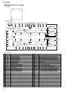
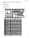
KS-LX200R
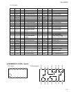
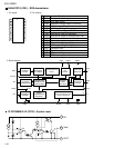
3. Pin function
1
2
3
4
5
6
7
8
9
10
11
12
13
14
15
16
17
18
19
20
21
22
23
24
IN1.2
OUT1
IN2.1
IN2.2
OUT2
IN3.1
IN3.2
OUT3
IN4.1
IN4.2
OUT4
CTL1
FWD1
REW1
CTL2
FED2
REW2
SGND
MUTE1
MUTE2
MUTE3
MUTE4
PVCC1
DO6.2
I
O
I
I
O
I
I
O
I
I
O
I
I
I
I
I
I
-
I
I
I
I
-
O
CH 1 op-amp input (-)
CH 1 op-amp output
CH 2 op-amp input (+)
CH 2 op-amp input (-)
CH 2 op-amp output
CH 3 op-amp input (+)
CH 3 op-amp input (-)
CH 3 op-amp output
CH 4 op-amp input(+)
CH 4 op-amp input (-)
CH 4 op-amp output
CH 5 motor speed
control
CH 5 forward input
CH 5 reverse input
CH 6 motor speed
control
CH 6 torward input
CH 6 reverse input
Signal ground
CH 1 mute
CH 2 mute
CH 3 mute
CH 4 mute
Power supply voltage
(For CH 5, CH 6)
CH 6 drive output
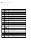
25
26
27
28
29
30
31
32
33
34
35
36
37
38
39
40
41
42
43
44
45
46
47
48
DO6.1
DO5.2
DO5.1
SO4.2
DO4.1
PGND
PGND
DO3.2
DO3.1
PGND
DO2.2
SO2.1
SO1.2
DO1.1
PVCC2
OPOUT
OPIN(-)
OPIN(+)
RES50
SVCC
REF
REG050
REG50
IN1.1
O
O
O
O
O
-
O
O
O
O
O
O
-
O
I
I
I
-
I
O
O
I
CH 6 drive outout
CH 5 drive output
CH 5 drive output
CH 4 drive output
CH 4 drive output
Power ground
Power ground
CH 3 drive output
CH 3 drive output
Power ground
CH 2 drive output
CH 2 drive output
CH 1 drive output
CH 1 drive output
Power supply voltage
(For CH 1, CH 2, CH 3, CH 4)
Opamp output
Opamp input (-)
Opamp input (+)
Regulator 5V reset
Signal supply voltage
Bias voltage input
regulator 5V output
Regulator output
CH 1 opamp onput (+)
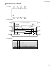
Pin No. Symbol I/O Function Pin No. Symbol I/O Function
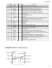
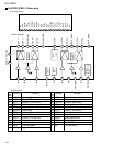
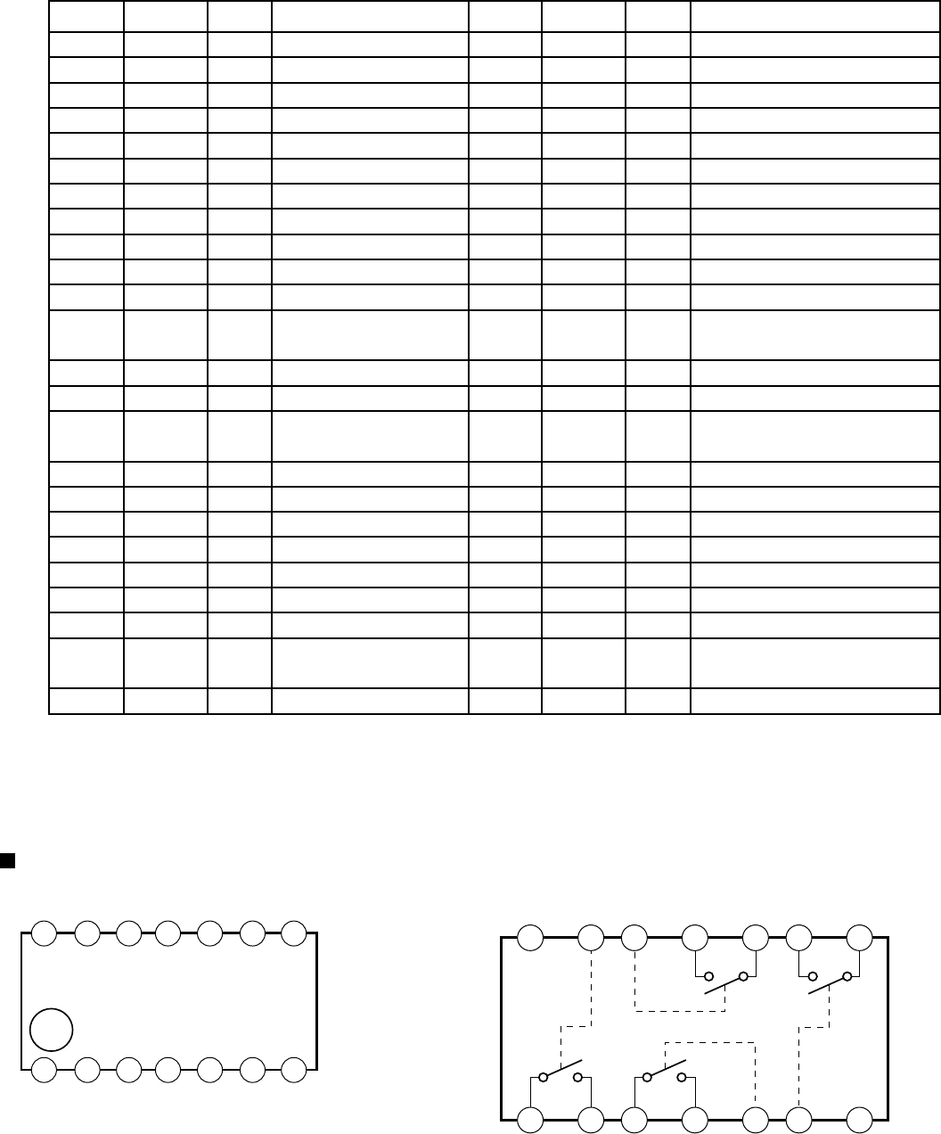
BU4066BCF-X (IC322) : Switch
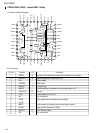
14 13 12 11 10 9 8
1 2 3 4 5 6 7
I/O 1
O/I 1
O/I 2
I/O 2
C2
C3
VSS
VDD
C1
C4
I/O 4
O/I 4
O/I 3
I/O 3
14 13 12 11 10 9 8
1 2 3 4 5 6 7
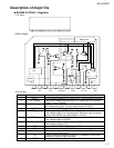
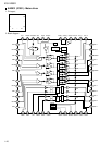
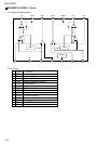
2.Block diagram
1.Pin l ayout