


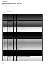

1-26
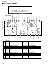
KS-LX200R
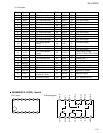
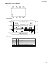
11
1
12
4
10
15
25
13
14
16
24
23
21
18
19
17
22
2
3
5
8
7
9
206
+
-
-
+
+
-
-
+
+
-
+
-
+
-
+
-
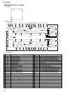
IN 1
TAB
IN 2
ST BY
R.F
IN 3
N.C
PRE GND
IN 4
ON TIME
PWR GND4
OUT 4-
OUT 4+
PWR GND3
OUT 3-
OUT 3+
MUTE
PWR GND2
OUT 2-
OUT 2+
PWR GND1
OUT 1-
OUT 1+
VCC3/4
VCC1/2
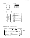
LA4743B (IC941) :Power amp
Muting &
on time control
circuit
Protective
circuit
Mute
circuit
Ripple
filter
Stand by
switch
Protective
circuit
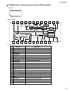
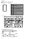
1 2 3 4 5 6 7 8 910111213141516171819202122232425
TAB
GND1
OUTFR+
STBY
OUTFR-
VCC1/2
OUTRR+
GND2
OUTRR-
VREF
INRR
INFR
SGND
INFR
INRL
ONTIME
OUTRL+
GND3
OUTRL-
VCC3/4
OUTFL+
MUTE
OUTFL-
GND4
NC
1.Terminal layout
2.Block diagram
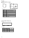
3.Pin function
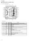
1
2
3
4
5
6
7
8
9
10
11
12
13
Header of IC
Power GND
Output (-) for front Rch
Stand by input
Output (+) for front Rch
Power input
Output (-) for rear Rch
Power GND
Output (+) for rear Rch
Ripple filter
Rear Rch input
Front Rch input
Signal GND
TAB
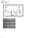
GND1
RFO-
STBY
RFO+
VCC1/2
RRO-
GND2
RRO+
R.F
RRIN
RFIN
SGND
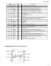
14
15
16
17
18
19
20
21
22
23
24
25
LFIN
LRIN
ONTIME
LRO+
GND3
LRO-
VCC3/4
LFO+
MUTE
LFO-
GND4
NC
Front Lch input
Rear Lch input
Power on time control
Output (+) for rear Lch
Power GND
Output (-) for rear Lch
Power input
Output (+) for front
Muting control input
Output (-) for front
Power GND
Non connection
Pin
No.
Symbol Function
Pin
No.
Symbol Function