


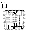

1-17
KS-LX200R
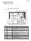
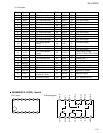
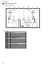
Description of major ICs
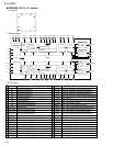
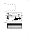
1234 56789101112
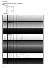
BA4905-V3 (IC961) : Regulator
1.Pin layout
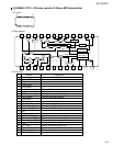
2.Block diagram
EXT
EXT ACC AUDIO 9V CTRL ILM 10V GND
RESET
RESET COMP VDD 5.7V CD 8V VCC AJ
1 2 3 4 5 6 7 8 9 10 11 12
37K
5K
REGULATOR
Overvoltage
protection circuit
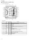
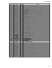
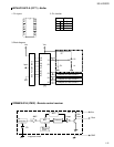
Pin no. Symbol Function
RESET
EXT output
COMP output
ACC
VDD output
AUDIO output
CD output
CTRL
VCC
ILM output
AJ
GND
1
2
3
4
5
6
7
8
9
10
11
12
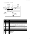
If VDD voltage becomes 4V or less.RESET output becomes low level.
This output voltage is approximately 0.5V lower than VCC. and max
output current is 300mA.
A voltage supply for ACC block. This output voltage is approximately
0.7V lower than VDD'S. The max output current is 100mA.
Control of the COMP output by inputting voltage.
This output voltage is 5.7V, and max output current is 100mA.
This voltage supply is for microcomputer. Whenever back up voltage
supply is connected, the output keeps on running.
This output voltage is 9.0v, and max output current is 500mA.
This voltage supply for AUDIO.
This output voltage is 8.0V, and max output current is 1A.
This voltage supply for CD.
Output selector of CD. AUDIO, ILM and EXT.
To be connected with the BACK UP of car.
This output voltage is 10V, and max output current is 500mA.
Output voltage is adjustable.
Putting a resistance between ILM and AJ or between AJ and GND
makes ILM output voltage adjustable.
Ground.
3.Pin function