


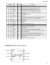
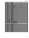
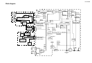
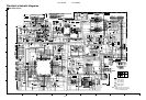
1-27
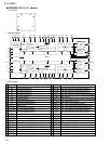
KS-LX200R
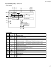
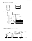
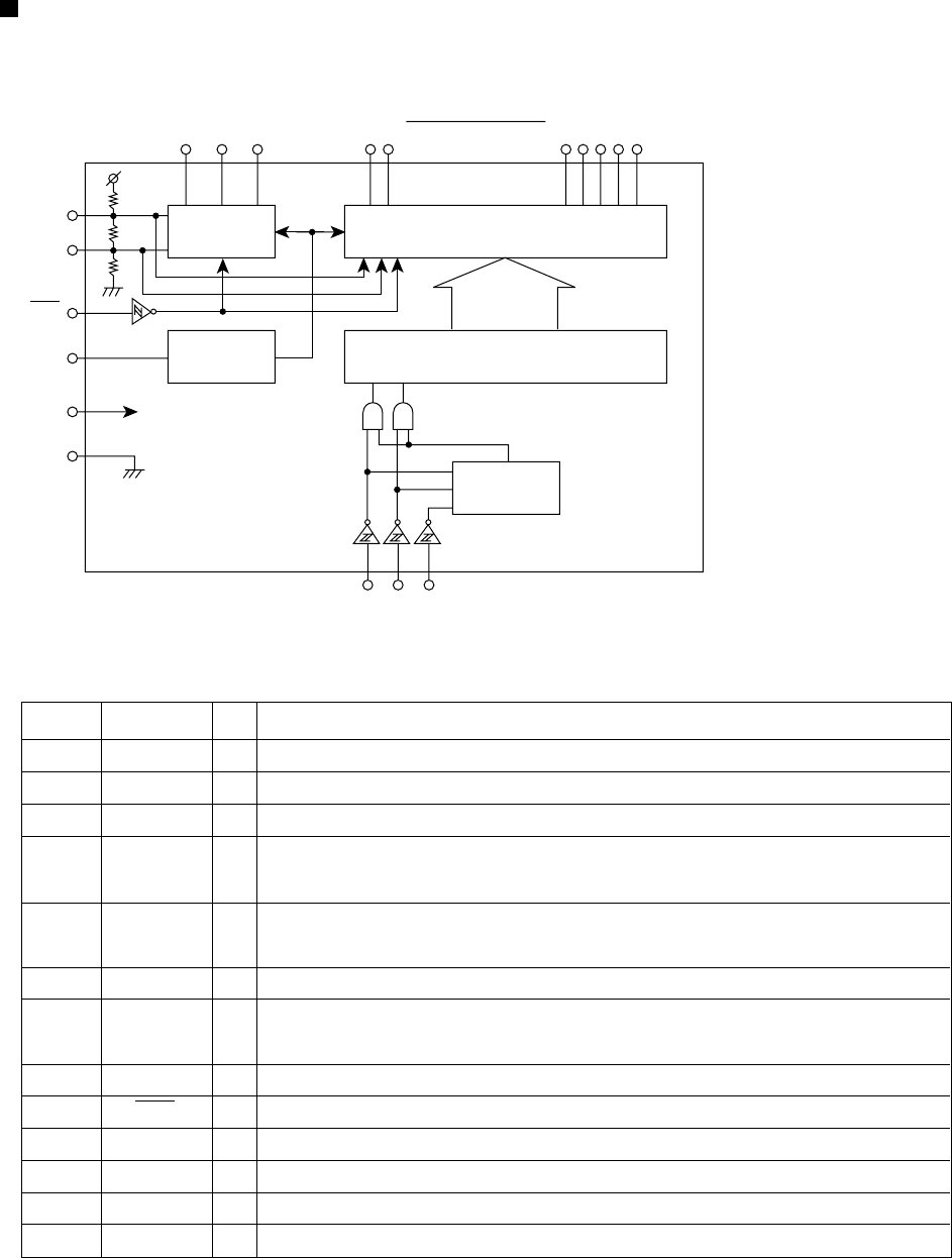
1.Block diagram
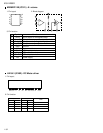
1~66
67~69
70
71
72
73
74
75
76
77
78
79
80
S3~S68
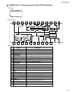
COM1~3
VDD
VDD1
VDD2
VSS
OSC
INH
CE
CLOCK
DI
S1
S2
Segment Output.
Common Driver Output.
Power Supply Connection.
Used for applying the LCD drive 2/3 bias voltage externally.
Must be connected to VDD2 when a 1/2 bias drive scheme in used.
Used for applying the LCD drive 1/3 bias voltage externally.
Must be connected to VDD1 when a 1/2 bias drive scheme in used.
Power supply connection.
Oscillator connection. An oscillator circuit is formed by connecting an
external resistor and capacitor to this pin.
Display off control input.
Chip enable input.
Synchronization clock input.
Serial data input.
Signal output.
Signal output.
O
O
-
I
I
-
I/O
I
I
I
I
O
O
Pin No. Symbol Description
I/O
2.Pin functions
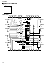
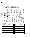
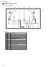
LC75873NW (IC601) : LCD driver
VDD1
VDD2
INH
OSC
VDD
VSS
COMMOM
DRIVER
CLOCK
GENERATOR
SEGMENT DRIVER
SHIFT REGISTER
ADDRESS
DETECTOR
COM3
COM2
COM1
S68
S67
S5
S4/P4
S3/P3
S2/P2
S1/P1