


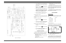
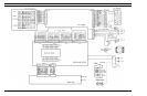

CONTROLLER CIRCUIT
This controller circuit consists of control circuits and
audio circuits. Physically, this circuit consists of three cir-
cuit boards as follows:
• Control Board
• Signaling Board
• LCD Board
Control Board
The Control board consists of the following circuits (see
Figure 2):
• CMOS Microcomputer (A1)
• RAM with Lithium Battery (A2 plus BT1)
• Audio Processor (A3)
• Audio Amplifier (A4, A6)
• Voltage Regulator Circuits (A7, A9, Q2, Q3, Q10 and
Q11)
• External Data Buffer (A5)
Microcomputer (A1):
The microcomputer provides various software for con-
trolling the radio unit as follows:
• Loading data to the frequency synthesizer
• Fetching and processing the PTT, monitor, channel se-
lection and volume control
• Loading data to the LCD display
• Controlling the audio circuit (Processor)
• Encoding/decoding the Channel Guard and digital
Channel Guard
• Controlling the loading interface for the radio data
(channel number and signaling)
RAM (A2):
RAM has a capacity of 2K bits X 8 for storing various
data for controlling the radio. The data is entered from the
outside to the microcomputer through the UDC connector
and then to the RAM. The data mainly consist of the follow-
ing:
• Channel Frequency Data
• CG/DCG data
• TX Power, TX Modulation Data
• Squelch Data
• Display Data ...etc.
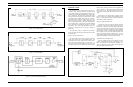
Audio Processor (A3):
The Audio processor consists of a one-chip IC accommo-
dating almost all of the audio functions. The audio functions
are under control of the microcomputer in compliance with
the function of the radio unit. The functions of the audio
processor are as follows:
• Tone Reject Filter
• Limiter Amplifier
• Volume and Modulation Level Control
• Post Limiter Filter
• Squelch Filter and Rectifier
• CG/DCG Encode/Decode Filter and Limiter
• D/A Converter and comparator
• OSC Circuit and Digital Interface for Microcomputer
All of these functions are made up of switched, capacitor
filters, amplifiers and timing logic. The timing for this logic
is derived from the 3.579545 MHz clock generator. The
clock signal is also applied to the microcomputer.
Audio Amplifier (A4 and A6):
The audio amplifier is located between the audio proces-
sor and the microphone or the speaker. Amplifier A6 pro-
vides pre-emphasis and amplification for transmit audio and
de-emphasis for the receive audio. Amplifier A4 amplifies
the output signal of A6 to the level adequate for driving the
speaker and VDC audio output.
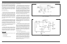
Voltage Regulator Circuits (A7, A9, Q2, Q3, Q10 and Q11):
Voltage Regulator Circuit A9 provides a regulated +2.5
VDC. Using the 2.5 VDC as a reference voltage, A9, Q2
and Q3, in combination, generate 5.4 VDC for the radio unit.
The control Transistors Q10 and Q11 are used for current-
limiting to avoid break down.
External Data Buffer (A5):
The External Data Buffer is located between the UDC
connector and the microcomputer for protection of the inter-
nal circuits.
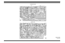
Signaling Board
The Signaling Board consists of the following circuits:
• CMOS Microcomputer (A301)
• Audio Amplifier (A302)
• Comparator (A303)
Microcomputer (A301):
The microcomputer provides various software for signaling
the radio unit as follows:
• Encoding the DTMF and GE Star
• Decoding the sequential Two Tone
• Providing control for SCAN operation
Audio Amplifier (A302):
The audio amplifier is located between the audio processor
and the microcomputer (A301). Amplifier (A302b and A302a)
provides a Low Pass Filter, resistors R310-R312 and capacitors
C303-C305, for tone encoding.
Comparator (A303):
The comparator converts the audio signal from the DISC
output into a signal which can decode the microcomputer
(A301).
LCD Board
The LCD board is composed of the following items:
• LCD Drive IC (A1)
• LCD
• Back Lighting Circuit (Q1, Q2 and CR1 - 6)
The LCD driver converts data from the microcomputer into
a signal which can drive the LCD display. The LCD display is
equipped with 8 character, 14 segments each and eight status
displays. Microcomputer signals drive the LCD driver and the
driver turns the LCD on. Also this board has a back 1ighting
circuit enabled upon receiving a signal from the microcom-
puter when any of the control switches (VOL, PTT, ...etc.) are
operated.
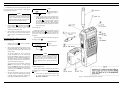
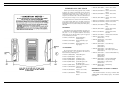
Key Pad
The key pad, used with the standard M-PD Personal Radio,
is located on the top of the housing. This key pad consists of
flexible cable and rubber contacts. The cable connects with the
microcomputer.
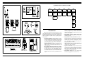
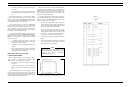
UDC Connector
The UDC connector is located on the side of the radio
housing so that various kinds of external equipment connec-
tions can be made. External equipment connecting signals are
as follows:
• TX Data
• RX Data
• CTS
• PTT
• EXT MIC
• RX Audio Out
• T/R
• Mute
• Disc Out
• +7.5 Volts
• Switch Out
• EMER
• UDC
The radio control microprocessor senses the value of volt-
age at the UDC line and switches the appropriate audio circuits
to provide proper radio/ accessory operation. The UDC volt-
age is set by two resistors within the UDC connector.
Battery Packs
The battery packs are available in three capacities: stand-
ard, high and extra high. All battery packs provide a nominal
7.5 Volt DC output.
To protect the battery pack from external short circuits, the
positive (+) charging contact is diode protected.
An internal thermistor senses variations in battery pack
temperature to automatically control a charger and provide a
maximum charge without overheating the battery pack. All
battery packs can be charged in one hour.
The battery is shipped fully charged to the customer, ready
for use. However, if the battery pack is stored for any length of
time it should be fully charged before placing into service.
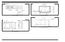
For Data Loader
For External MIC
& SPKR
GE Star Lanyard
LBI-31629
8