


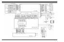

Q202. The RF power output from Pin 2 of the TX-Amp
module A201 is connected through a resistor attenuator to
Pin 1 of the PA module where it is applied to the input of the
RF power amplifier stages. The RF power amplifier stages
amplify the input from the TX-Amp module to a typical
power output level of 6 watts at Pin 5. The output at Pin 5 is
connected through the power control hybrid IC A203 (PC)
and TX-RX switching diode CR201 to low pass filter net-
work FN. A minimum power level of 5 watts is on the out-
put of the filter network.
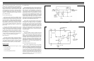
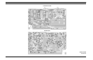
Power Control Module (A203):
The RF power output of the radio is regulated by sensing
variations in the RF power output of the transmit PA module
to control the supply voltage to the first stage of the PA mod-
ule (refer to Figure 5). Supply voltage cannot be applied to
the first stage of the PA module until the transmit circuit is
keyed, applying 5.4 Volts to Pin 11 of Power Control (PC)
hybrid IC A203. When the transmit circuit is keyed, the out-
put of a reference amplifier, determined by the High-Low
power control, is applied to the positive (+) input of a com-
parator circuit.
The output of the final PA is connected to Pin 1 of the
PC module and to the 50 ohm coupled line. The detected
voltage of the CM coupled output is applied to the negative
(-) input of the comparator circuit. The amplifier is enabled
when the transmit circuit is keyed, until then, the output of
the amplifier is low and transistor Q202 is held off. As the
PA module begins to increase output power, the detected
voltage causes the series regulator circuit to regulate the sup-
ply voltage to maintain constant RF output power.
Filter Network (FN):
The output of the PA module is connected to filter net-
work FN through TX-RX switching diode CR201. The FN
network is a passive LC low pass filter with an insertion loss
of less than 0.5 dB in the pass band. It also has a rejection
greater than 45 dB in the stop band. The output of the FN is
connected to the system antenna or to the UDC connector.
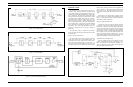
Receive Circuit
The M-PD receive circuit, as shown in Figure 2, consists
of the following circuits:
• RF Amplifier/Mixer
• First IF Amplifier
• Second IF Amplifier/Discriminator
RF Amplifier/Mixer:
The RF Amplifier/Mixer circuit contains two third order
band pass filters (FL301 and FL302), an RF amplifier circuit
(Q301) and a double balanced diode mixer circuit (A301).
Refer to Figure 6 - RF Amplifier/Mixer. RF from the an-
tenna or UDC connector is coupled through transmit low
pass filter FN and RF switching diode CR201 to the input of
the RF amplifier circuit. Low pass filter FN is used in the
receive circuit to provide additional receive selectivity. The
RF signal on the input of the RF amplifier is first coupled
through band pass filter FL301 to the input of grounded
emitter, broad band RF amplifier transistor Q301. This am-
plifier provides 12 dB of power gain to reduce thermal noise.
The output of the RF amplifier is coupled through band pass
filter FL302 to drive double balanced mixer A301.
The RF signal from the RF amplifier and the injection
frequency from the synthesizer circuit, provide a difference
of 45 MHz IF on the output of the mixer. The double bal-
anced Mixer has a typical conversion loss of 6 dB between
the RF input and IF output. All inputs and the output of the
RF Amplifier/Mixer one 50 ohms impedance. The +7 dBm
injection frequency level, provided by the synthesizer and
amplifier circuit transistor Q106, is connected to the injec-
tion frequency input through a 50 ohms matching circuit.
The output of the Mixer circuit is connected to the input of
the first IF Amplifier.
First IF Amplifier:
The first IF amplifier contains two amplifier circuits and
two crystal filters of two and four poles respectively (refer to
Figure 7). The first IF signal (45 MHz) from the first mixer
circuit connects to the input of pre-amplifier transistor Q302
through pre-crystal filter FL303 with an impedance of ap-
proximately 3K ohms. Pre-amplifier Q302 provides a 17 dB
power gain. The output is connected to the input of IF am-
plifier transistor Q303 through crystal filter FL304. IF am-
plifier Q303 has a 13 dB power gain, an input impedance of
approximately 3K ohms and an output impedance of ap-
proximately 2.2K ohms.
Second IF Amplifier/Discriminator (A302):
The Second IF Amplifier/Discriminator circuit contains
FM IF IC A302 (HA12442V) and 455 kHz ceramic filter
FL305 (refer to Figure 8). The FM IF IC contains a local os-
cillator, mixer, IF amplifier, FM detector and an audio ampli-
fier. The 45 MHz IF output from the first IF amplifier is
connected to the input of second IF amplifier A302a, Pin 2
of HA12442V and converted to the second IF frequency
(455 kHz). The second IF output is connected to Pin 7 of
HA12442V through the 455 kHz ceramic filter to the IF am-
plifier and FM detector circuits. The recovered audio from
the FM IF IC is connected to J102-4.
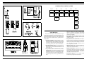
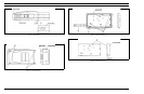
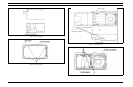
Figure 4 - Power Amplifier
Figure 5 - Power Control Module
LBI-31629
6