


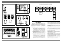
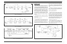
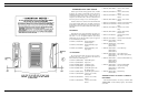
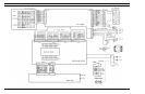

Synthesizer Circuit
The Synthesizer circuit contains Phase-Lock-loop mod-
ule (PLL) A102, VCTCXO Reference Oscillator module
A103, TX/RX Voltage Controlled Oscillator module (VCO)
A106 and a Low Pass Filter amplifier (LPF). Refer to Fig-
ure 9 - Synthesizer. The VCO used to generate the receive
and transmit reference frequencies is phase locked to a stable
VCTCXO reference oscillator through the use of the PLL.
This feedback loop divides the VCO frequency down to a
signal in the range of 7 MHz - 10 MHz; divides this signal
with a programmable divider to 5/6.25 kHz and generates a
VCO control signal by comparing the 5/6.25 kHz feedback
with a 5/6.25 kHz signal derived by dividing a 13.5 MHz
VCTCXO by 1056. As the least significant bit in the pro-
gramming is changed, the VCO is forced to change by
5/6.25 kHz.
The synthesizer circuitry is contained on two modules,
the VCO module A106 and the VCTCXO reference Oscilla-
tor module A103.
Phase-Lock-Loop Module (A102):
The PLL module A102 contains a reference frequency,
divider, phase detector and a programmable divider. The
phase detector DC voltage output signal is filtered with a
passive low pass filter followed by a 6.25 kHz filter to re-
duce the level of reference modulation on the VCO. This
DC output represents the error between the VCO frequency
(phase) and the reference (VCTCXO) and is applied to the
VCO on frequency. A lock detect output is developed from
Pin 9 output of A102. This output is checked by the micro-
computer to prevent transmission before the VCO is on fre-
quency.
Serial data from the microcomputer is shifted into the
PLL to set the division parameter which establishes the fre-
quency. A clock signal is provided on another input and the
data is latched with the enable input.
Voltage Controlled Oscillator A106:
The VCO uses a low noise, high gain transistor as the ba-
sic oscillator. The resonant circuit, which determines the
frequency of oscillation, is formed by a High Q coil which is
used to set the center frequency at the factory. The output of
each VCO (TX and RX) is coupled into a cascade amplifier
which produces +3 dBm. The output of the RX-VCO ampli-
fier is coupled into the receive first double balanced mixer
circuit A301 through buffered amplifier Q106. The TX-
VCO amplifier output is directly connected to the TX-Amp
input through attenuator circuit R201, R202 and R203.
VCTCXO Reference Oscillator A103:
The A103 oscillator module is self contained, fully tem-
perature compensated and operates at a frequency of 13.2
MHz. The oscillator also has modulation capability. Fre-
quency is adjusted by a trimmer while monitoring the trans-
mit circuit output at the antenna jack.
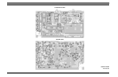
Figure 6 - RF Amplifier/Mixer
Figure 7 - First IF Amplifier
Figure 8 - Second IF Amplifier/Discriminator
Figure 9 - Synthesizer
LBI-31629
7