


2
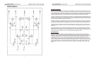
VOLTAGE AMPLIFIER:
The voltage amplifier amplifies the audio signal?s voltage from 4.8 volts peak (at the output of U2) to approximently
97v peak which is required to drive the current amplifier board M1002A. M1002A provides the current required for the
97v peak signal to drive 1200 watts into 4 ohms out of the binding posts.
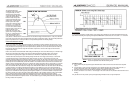
Before the circuit is described in detail here is a quick rundown on the signal?s path through the voltage amplifier
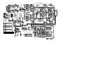
stage. Refer to the schematic of M1011A. Let's consider that a positive going AC signal is present @ test point 3. The
positive going signal will turn on the positive side of the voltage amplifier. The signal at test point 3 turns on Q12
(through R40, D14 and D13). The collector of Q12 pulls down on the base of Q14, turns this transistor on further and
allows a greater current to flow out of Q14?s collector. This increase in current passes through Q15 and it?s collector to
emitter voltage drop decreases. The collector of Q15 now being more positive in voltage turns the base of Q18 on
causing an increase in Q18?s collector current resulting in test point 5 going positive.
As the positive side of the amplifier was turning on the negative side would have been turning off. This is how test
point 5 was able to move positive following the input signal. The reverse would hold true if a negative going signal was
present on the input of the voltage amplifier.
CIRCUIT DESCRIPTION:
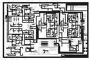
The voltage amplifier is a mirrored image with circuitry connected to the positive power supply rail being identical (but
opposite polarity) to the circuitry connected to the negative power supply rail.
For this reason we will look in detail at the positive side of the amplifier.
The audio signal enters the voltage amplifier at test point 3. The signal passes through R40, D14 and D13 to the base
of Q12. Diodes D13 and D14 set up the DC bias on Q12 to approximately 0.6 mA.
The first voltage gain stage consists of Q12 along with the resistor chain on its collector and the emitter resistor (R44).
Transistor Q12 drives the base of Q14 through the resistor chain. A DC current of approximately 6 mA should flow
through the collector of Q14. The voltage drop across Q14 remains constant and is derived from the voltage drop
across the voltage reference Q20, resistor R58, and the base/emitter junction of Q15. This total voltage should equal
approximately 3 VDC. Transistor Q14 is the second gain stage and its output current flows through Q15. Transistor
Q15 is a common base stage with the collector driving the base of output buffer Q18.
Diode D17 is a clamping diode that prevents the maximum peak of the audio signal from coming within 4V of the 144
VDC rail. This is to prevent the output current amplifier (board M1002A) from going into saturation during clipping and
therefore having storage delay problems.
Transistor Q18 buffers the high impedance present on the collector of Q15. The output of the buffer provides a low
output impedance at test point 5 and is current limited to 25mA through the clamping action of D19, D20 and D23.
The signal at TP-5 drives the current amp board M1002A.
DC offset on the amplifier?s output is corrected by operational amplifier U2. The DC offset forms a current through
R54, R14 and is blocked by C5 giving a DC offset correction gain of -1.
The activity L.E.D. function is a simple charge pump circuit with a transistor that redirects a constant current path
through the activity L.E.D.
3
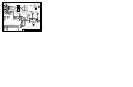
SHUTDOWN CIRCUIT:
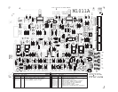
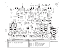
The last circuit on board M1011A is the shutdown relay and its associated drive circuitry. The relay circuit has two
possible operating states.
1.
Amplifier on under normal operating conditions.
2.
Amplifier power switch has just been turned OFF/ON or the amplfier is in current limit protecting the amplifier?s
output or the amplifier has overheated.
CIRCUIT DESCRIPTION
Here is how the circuit accomplishes these functions. The relay?s normally closed contacts short the output of the
voltage amplifiers to ground when the power switch is off. When the power switch is turned on, the relay remains off
(normally closed) for about 6 seconds. C52 charges to 35V and results in Q37 turning off allowing Q36 to turn on. As
Q36 turns on, it connects the negative terminal of the relay?s coil (Pin 16) to ground energizing the relay and opening
the normally closed contacts.
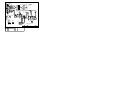
If prolonged current limiting occurs on the amplifier?s output transistors then D50 or D51 (depending on which channel
is current limiting) will be forward biased turning on Q38 (from its off state). Now +144VDC appears on the collector of
Q38 and through R130 and R128 turn on Q37 therefore turning off Q36 by shorting its base emitter junction. Q36
turning off will turn the relay off and the normally closed contacts (off state) will short the outputs of the voltage
amplifiers to ground so as not to continuously stress the amplifier?s output transistors. A cycle now occurs. With the
voltage amplifiers now disabled there is no signal driving the output transistors (Q14 to Q28) on board M1002A.
The current limit circuit on M1002A turns off and D50 and/or D51 are not forward biased and Q38 turns off. Through
Q37 and Q36 the relay is turned back on and the voltage amplifiers are now active again, driving the output
transistors. If current limiting still occurs, then the same cycle will occur. If the cause of current limiting (low impedance
or short on the speaker output terminals) has been removed, then the amplifier will continue to operate normally.
The third operation that the relay provides is "overheat shutdown". If for some reason the fan cannot keep the
heatsinks in a safe operating temperature area then the fan control circuit (on board M1013A) will deliver through the
"kill" signal line a positive current to turn Q37 on and turn Q36 off to turn off the relay and disable the voltage
amplifiers. When the temperature of the amplifier has been cooled down by the fan, then the kill signal will disappear
and the relay circuit will turn on the relay to resume normal operation. Anytime the relay is in the "protect" mode (due
to the abnormal states) then contact pin 8 of the relay will illuminate LD5 (the protect LED on the front panel).
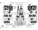
M1002A “CURRENT AMPLIFIER BOARD”
The current amplifier board (M1002A) receives a high voltage audio signal from voltage amplifier board (M1011A) and
provides the current drive necessary to drive speaker cabinets.
The current amplifier is a two tier complimentary output driver design controlled by a complimentary mos-fet stage.
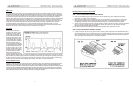
CIRCUIT DESCRIPTION - REFER TO THE SIMPLIFIED SCHEMATIC #1 ON THE FOLLOWING PAGE