


STR-DE835/DE935/SE591/V828
— 11 — — 12 —
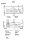
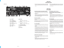
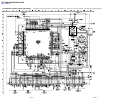
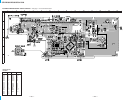
SP board
V-SWITCH board
VIDEO board
S-VIDEO board
DIGITAL board
JOINT(H) board
MAIN board
VOLUME board
MUTING board
REAR-AMP board
ROTARY board
LED board
SW board
H.P board
SP-SW board
DISPLAY board
DC board
AC board
4/8 board
TUNE
R
board
4-3. CIRCUIT BOARD LOCATION
For schematic diagrams.
Note:
• All capacitors are in µF unless otherwise noted. pF: µµF
50 WV or less are not indicated except for electrolytics
and tantalums.
• All resistors are in Ω and
1
/
4
W or less unless otherwise
specified.
• % : indicates tolerance.
• 2 : nonflammable resistor.
• 1 : fusible resistor.
• C : panel designation.
• U : B+ Line.
• V : B– Line.
• H : adjustment for repair.
• Voltages and waveforms are dc with respect to ground
under no-signal (detuned) conditions.
No mark : FM
• Voltages are taken with a VOM (Input impedance 10 MΩ).
Voltage variations may be noted due to normal production
tolerances.
• Waveforms are taken with a oscilloscope.
• Circled numbers refer to waveforms.
• Signal path.
F : FM
J : CD
c : DIGITAL
I : PHONO
• Abbreviation
CND :Canadian model
AUS :Australian model
MY :Malaysia model
SP :Singapore model
CH :Chinese model
THIS NOTE IS COMMON FOR PRINTED WIRING
BOARDS AND SCHEMATIC DIAGRAMS.
(In addition to this necessary note is printed in each
block.)
Note:
The components identified by
mark ! or dotted line with mark
! are critical for safety.
Replace only with part number
specified.
Note:
Les composants identifiés par
une marque ! sont critiques
pour la sécurité.
Ne les remplacer que par une
pièce portant le numéro spécifié.
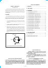
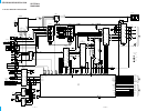
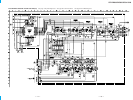
• Waveform
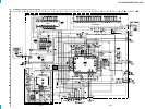
DIGITAL Board
1 IC1201 (™ (XO)
2 IC1401 (CLKO)
3 IC1404 25
4.0Vp-p
3.5Vp-p
5.5Vp-p
4MHz
10MHz
12.288MHz
100
DISPLAY Board
4 IC102 *™ (XO)
5 IC12 !§ (X OUT)
3.6Vp-p
3.8Vp-p
16.0MHz
7.28MHz
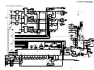
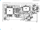
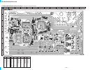
For printed wiring boards.
Note:
• X : parts extracted from the component side.
• ® : Through hole.
• b : Pattern from the side which enables seeing.