


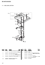
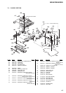
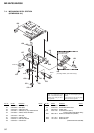
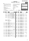
44
MZ-NH700/NHF800
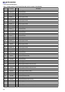
Pin No. Pin Name I/O Description
195 SI0 I Serial data input from the EEPROM
196 SO0 O Serial data output to the EEPROM, A/D converter and controllers
197 SCK0 O Serial clock output to the EEPROM, A/D converter and controllers
198 XGUM_ON I Rechargeable battery detection signal input terminal Not used
199 BEEP O Beep sound control signal output to the headphone amplifier
200 XOPT_CTL O Power supply on/off control signal output for the optical input jack
201 LAM_REQCHK I LAM power check terminal Not used
202 LAM_SPREQ O LAM force stop request signal output Not used
203
REC_LED
/ACCESS_LED
O REC or Access LED drive signal output terminal Not used
204 MDVCC_CTL O Power supply control signal output for the OP modulation
205 VBUS_VB_CTL O USB power supply control signal output terminal
206 LAM_NAME O LAM name data request signal output terminal Not used
207 DRAM_ALONE O Self-refresh signal output for internal D-RAM
208 PF0 — Not used
209 PF1/S0DO O Connect to the optical pick-up block
210 PF2/S1DO O Connect to the optical pick-up block
211 PF3/RTG3 O Connect to the headphone amplifier
212
XMUTE
/MUTE
O Muting on/off control signal output terminal
213 SI1 I Serial data input from the LCD module
214 SO1 O Serial data output to the LCD module
215 SCK1 I/O Serial data transfer clock signal input/output terminal with the LCD module
216 SLD_MON I Sled servo monitoring terminal
217 AOUT_SEL O Headphone/line output switching terminal Not used
218 YUZU_SLEEP O Chip enable output to the power control IC
219 FFCLR O Power on/off control signal output for FCRAM (internal RAM)
220 CHGI_CTL1 O
Charge current limiter control signal output at the time of DC adaptor use
“L”: charge Not used
221 CHGI_CTL2 O Charge current control signal output terminal “L”: low current charge
222 CHGI_CTL3 O Charge current control signal output terminal “L”: low current charge
223 SLBUSY I Receive signal monitoring terminal for sled command
224 XTEST I Terminal for the test mode setting (normally open) “L”: test mode
225 XRF_RST O Reset signal output to the RF amplifier
226 VREC_SEL O VREC start-up timing control signal output terminal
227 XHOLD_SW I HOLD switch detection input terminal
228 T_MARK_SW I Track mark switch input terminal Not used
229 XRST2_DET I Reset signal input from the power control IC
230 CHGI_SEL O Charge/discharge control signal output for current sense amplifier Not used
231 RECP_MON I Laser power changeover signal monitoring terminal
232 SPDL_MON I Spindle servo monitoring terminal
233 XCS_PWR_IC O Chip select signal output to the power control IC
234 RXD I Not used
235 TXD O Not used
236 XCS_LCD O Chip select signal output to the LCD module
237
CC_CTL
/VI_CTL
O Constant current circuit control signal output terminal