


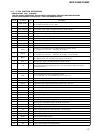
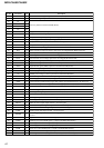
46
MDX-CA680/CA680X
Pin No. Pin Name I/O Description
46 LINKOFF O
Unilink on/off control signal output for the SONY bus “L”: link on, “H”: link off
47 UNIREQ O
Data request signal output terminal (for SONY bus) “H”: request on Not used (open)
48 UNICKIO I/O
Serial clock signal input from the system controller (IC501) or serial clock signal output to the
SONY bus interface (IC505) and system controller (IC501) (for SONY bus)
49 UNISI I
Serial data input from the SONY bus interface (IC505)
50 UNISO O
Serial data output to the SONY bus interface (IC505)
51 MD-CKO O
Serial data transfer clock signal output to the CXD2662R (IC301) and CXA2523AR (IC302)
52 MD-SI I
Reading serial data signal input from the CXD2662R (IC301)
53
—
O
Not used (open)
54 SENS I
Internal status (SENSE) input from the CXD2662R (IC301)
55 CC-XINT
I Interrupt status input from the CXD2662R (IC301)
56 LIMIT-IN
I
Detection input from the sled limit-in detect switch
The optical pick-up is inner position when “L”
57 EJT-OK I
Front panel open detection signal input terminal “L”: eject possible
58 ERROR-PWM O
PWM error monitor output terminal (C1and ATER is output when test mode) Not used (open)
59 MD-RST O
Reset signal output to the PCM1718E (IC101), CXD2662R (IC301) and BH6518FS (IC303)
“L”: reset
60 BU-IN I
Battery detect signal input from the SONY bus interface (IC505) and battery check circuit
“H”: battery on
61 BUS-ON I
SONY bus on/off control signal input from the system controller (IC501) “L”: bus on
62 SQSY
I
Subcode Q sync (SCOR) input from the CXD2662R (IC301)
“L” is input every 13.3 msec Almost all, “H” is input
63 C-SW I
Inputs a disc loading start or a disc eject completion detect switch detection signal
“L”: When loading start or eject completed of a disc loading operation
64 MD-LAT O
Serial data latch pulse signal output to the CXD2662R (IC301) and CXA2523AR (IC302)
65 MD-ON O
Power supply on/off control signal output of the MD mechanism deck section main power supply
“H”: power on
66 DEEMP O
De-emphasis on/off control signal output to the PCM1718E (IC101) “H”: de-emphasis on
67 A-MUTE O
Audio muting on/off control signal output
68 — O
Not used (open)
69 TSTCKO O
Output of clock signal for the test mode display Not used (open)
70 TSTSO O
Output of data for the test mode display Not used (open)
71 TSTMOD I
Setting terminal for the test mode “L”: test mode, “H”: normal mode
72 VCC —
Power supply terminal (+5V)
73 NC I
Not used (fixed at “H”)
74 to 77
TOUT0 to TOUT3
O
Output of the 4×8 matrix test keys Not used (open)
78 to 80 TIN0 to TIN2 I/O
Input of the 4×8 matrix test keys (“L” is always output, except in test mode) Not used (open)