


45
MDX-CA680/CA680X
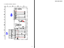
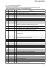
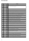
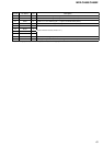
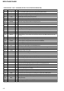
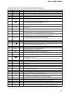
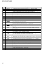
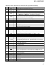
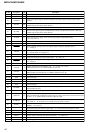
• SERVO BOARD IC501 CXP84340-231Q (MD MECHANISM CONTROLLER)
Pin No. Pin Name I/O Description
1 to 5 TIN3 to TIN7 I/O
Input of the 4×8 matrix test keys (“L” is always output, except in test mode) Not used (open)
6LOAD
O Loading motor control signal output to the motor driver (IC305) “H” active *1
7 EJECT O
Loading motor control signal output to the motor driver (IC305) “H” active *1
8, 9
—
O
Not used (open)
10 MDMON O
Power supply on/off control signal output of the MD mechanism deck section main power supply
and loading motor drive (IC305) power supply “H”: power on
11 E-SW I
Inputs a disc loading completion detect switch detection signal
“L”: When completed of a disc loading operation
12 AG-OK O
Output of aging status in test mode “L”: under aging, “H”: aging completed Not used (open)
13 ADJ-OK O
Output of status when aging completed in test mode “L”: aging NG, “H”: aging OK
Not used (open)
14 to 17
—
O
Not used (open)
18 DFCTSEL I
Select whether defect function is used for the CXD2662R (IC301)
“L”: used this function , “H”: not used this function (fixed at “H” in this set)
19 DPLLSEL I
Select whether double PLL function is used for the CXD2662R (IC301)
“L”: used this function , “H”: not used this function (fixed at “H” in this set)
20 EMPHSEL I
Select whether emphasis signal output from pin or unilink data
“L”: outputs from both pin and unilink data, “H”: output from pin only (fixed at “H” in this set)
21 LOCK O
Mini-disc lock detection signal output terminal Not used
22
—
O
Not used (open)
23 2M/4M I
Select whether D-RAM capacitance 2M bit or 4M bit “L”: 4M bit (external D-RAM) , “H”: 2M
bit (internal D-RAM of CXD2652AR) (fixed at “L” in this set)
24, 25
—
O
Not used (open)
26
MNT0
I
Focus OK signal input from the CXD2662R (IC301)
“H” is input when focus is on (“L”: NG)
27 MNT1 I
Track jump detection signal input from the CXD2662R (IC301)
28 MNT2 I
Busy monitor signal input from the CXD2662R (IC301)
29 MNT3 I
Spindle servo lock status monitor signal input from the CXD2662R (IC301)
30 RESET I
System reset signal input from the system controller (IC501), reset signal generator (IC602) and
reset switch (S702) “L”: reset
For several hundreds msec. after the power supply rises, “L” is input, then it changes to “H”
31 EXTAL
I Main system clock input terminal (10 MHz)
32 XTAL
O Main system clock output terminal (10 MHz)
33 VSS
— Ground terminal
34 TX
O Sub system clock output terminal (32.768 kHz) Not used (open)
35 TEX
I Sub system clock input terminal (32.768 kHz) Not used (fixed at “L”)
36 AVSS
— Ground terminal (for A/D converter)
37 AVREF
I Reference voltage input terminal (+5V) (for A/D converter)
38 INIT
I Initial reset signal input terminal (A/D input) (fixed at “H”)
39 TEMP
I Temperature sensor (TH501) input terminal (A/D input)
40 ACNT
I
Select the number of load/eject aging times (A/D input)
0h – 54h (30 times), 55h – 0A9h (20 times), 0AAh – 0FFh (10 times)
41 DO-SEL
I Select the digital output bits (A/D input)
42 EE-CS
O Chip select signal output to the external EEPROM device Not used (open)
43 EE-CKO
O Serial data transfer clock signal output to the external EEPROM device Not used (open)
44 EE-SIO I/O
Two way data bus with the external EEPROM device Not used (open)
45 MD-SO O
Writing serial data signal output to the CXD2662R (IC301) and CXA2523AR (IC302)