


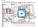
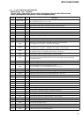
42
MDX-CA680/CA680X
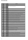
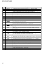
Pin No. Pin Name I/O Description
46 XRAS O Row address strobe signal output to the D-RAM (IC307) “L” active
47 XWE O Write enable signal output to the D-RAM (IC307) “L” active
48 D1 I/O
49 D0 I/O
50 D2 I/O
51 D3 I/O
52 MVCI
I
Digital in PLL oscillation input from the external VCO Not used (fixed at “L”)
53 ASYO O Playback EFM full-swing output terminal
54 ASYI I (A) Playback EFM asymmetry comparator voltage input terminal
55 AVDD — Power supply terminal (+3.3V) (analog system)
56 BIAS I (A) Playback EFM asymmetry circuit constant current input terminal
57 RFI I (A) Playback EFM RF signal input from the CXA2523AR (IC302)
58 AVSS — Ground terminal (analog system)
59 PCO O (3) Phase comparison output for master clock of the recording/playback EFM master PLL
60 FILI I (A) Filter input for master clock of the recording/playback master PLL
61 FILO O (A) Filter output for master clock of the recording/playback master PLL
62 CLTV I (A) Internal VCO control voltage input of the recording/playback master PLL
63 PEAK I (A) Light amount signal (RF/ABCD) peak hold input from the CXA2523AR (IC302)
64 BOTM I (A) Light amount signal (RF/ABCD) bottom hold input from the CXA2523AR (IC302)
65 ABCD I (A) Light amount signal (ABCD) input from the CXA2523AR (IC302)
66 FE I (A) Focus error signal input from the CXA2523AR (IC302)
67 AUX1 I (A) Auxiliary signal (I
3
signal/temperature signal) input from the CXA2523AR (IC302)
68 VC I (A) Middle point voltage (+1.65V) input from the CXA2523AR (IC302)
69 ADIO O (A) Monitor output of the A/D converter input signal Not used (open)
70 AVDD — Power supply terminal (+3.3V) (analog system)
71 ADRT I (A) A/D converter operational range upper limit voltage input terminal (fixed at “H” in this set)
72 ADRB I (A) A/D converter operational range lower limit voltage input terminal (fixed at “L” in this set)
73 AVSS — Ground terminal (analog system)
74 SE I (A) Sled error signal input from the CXA2523AR (IC302)
75 TE I (A) Tracking error signal input from the CXA2523AR (IC302)
76 DCHG I (A) Connected to the +3.3V power supply
77 APC I (A) Error signal input for the laser automatic power control Not used (fixed at “L”)
78 ADFG
I
ADIP duplex FM signal (22.05 kHz ± 1 kHz) input from the CXA2523AR (IC302)
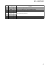
79 F0CNT O Filter f0 control signal output terminal Not used (open)
80 XLRF O Serial data latch pulse signal output terminal Not used (open)
81 CKRF O Serial data transfer clock signal output terminal Not used (open)
82 DTRF O Writing serial data output terminal Not used (open)
83 APCREF O
Control signal output to the reference voltage generator circuit for the laser automatic power
control
84 TEST0 O Input terminal for the test Not used (open)
85 TRDR O Tracking servo drive PWM signal (–) output to the BH6518FS (IC303)
86 TFDR O Tracking servo drive PWM signal (+) output to the BH6518FS (IC303)
87 DVDD — Power supply terminal (+3.3V) (digital system)
88 FFDR O Focus servo drive PWM signal (+) output to the BH6518FS (IC303)
89 FRDR O Focus servo drive PWM signal (–) output to the BH6518FS (IC303)
90 FS4 O Clock signal (176.4 kHz) output terminal (X’tal system) Not used (open)
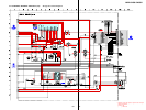
Two-way data bus with the D-RAM (IC307)