


TZA3046_1 © Koninklijke Philips Electronics N.V. 2006. All rights reserved.
Product data sheet Rev. 01 — 19 May 2006 5 of 15
Philips Semiconductors
TZA3046
Fiber Channel/Gigabit Ethernet transimpedance amplifier
The parasitic capacitance can be minimized through:
1. Reducing the capacitance of the PIN diode. This is achieved by proper choice of PIN
diode and typically a high reverse voltage.
2. Reducing the parasitics around the input pad. This is achieved by placing the PIN
diode as close as possible to the TIA.
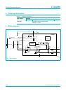
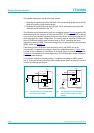
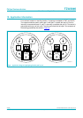
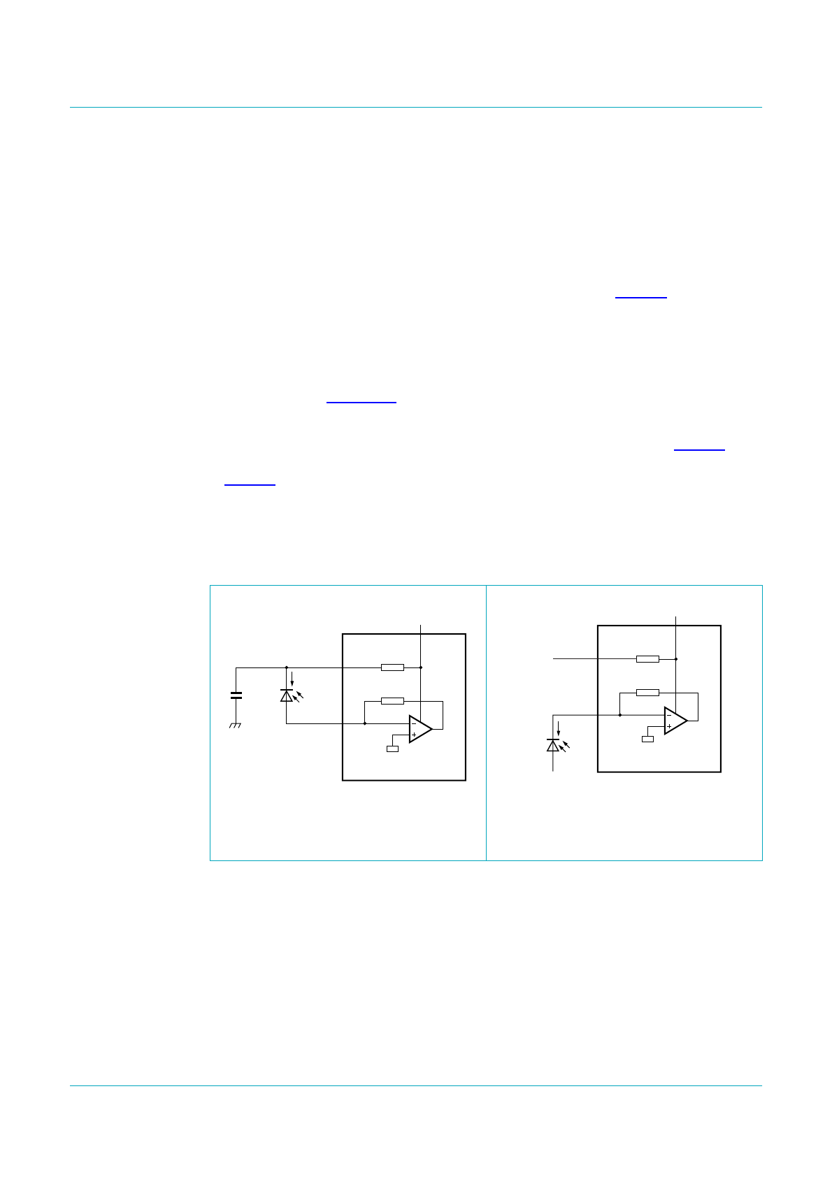
The PIN diode can be biased with a positive or a negative voltage. Figure 3 shows the PIN
diode biased positively, using the on-chip bias pad DREF. The voltage at DREF is derived
from V
CC
by a low-pass filter comprising internal resistor R
DREF
and external capacitor C2
which decouples any supply voltage noise. The value of external capacitor C2 affects the
value of PSRR and should have a minimum value of 470 pF. Increasing this value
improves the value of PSRR. The current through R
DREF
is measured and sourced at pad
IDREF_MON, see Section 7.3.
If the biasing for the PIN diode is done external to the IC, pad DREF can be left
unconnected. If a negative bias voltage is used, the configuration shown in Figure 4 can
be used. In this configuration, the direction of the signal current is reversed to that shown
in Figure 3. It is essential that in these applications, the PIN diode bias voltage is filtered to
achieve the best sensitivity.
For maximum freedom on bonding location, 2 outputs are available for DREF (pads 1
and 3). These are internally connected. Both outputs can be used if necessary. If only one
is used, the other can be left open.
Fig 3. The PIN diode connected between
the input and pad DREF
Fig 4. The PIN diode connected between
the input and a negative supply
voltage
001aae513
R
DREF
290 Ω
C2
470 pF
DREF
I
PIN
IPHOTO
4 or 17
1 or 3
2
TZA3046
V
CC
001aae514
R
DREF
290 Ω
DREF
negative
bias voltage
I
PIN
IPHOTO
4 or 17
1 or 3
2
TZA3046
V
CC