


TZA3046_1 © Koninklijke Philips Electronics N.V. 2006. All rights reserved.
Product data sheet Rev. 01 — 19 May 2006 12 of 15
Philips Semiconductors
TZA3046
Fiber Channel/Gigabit Ethernet transimpedance amplifier
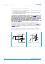
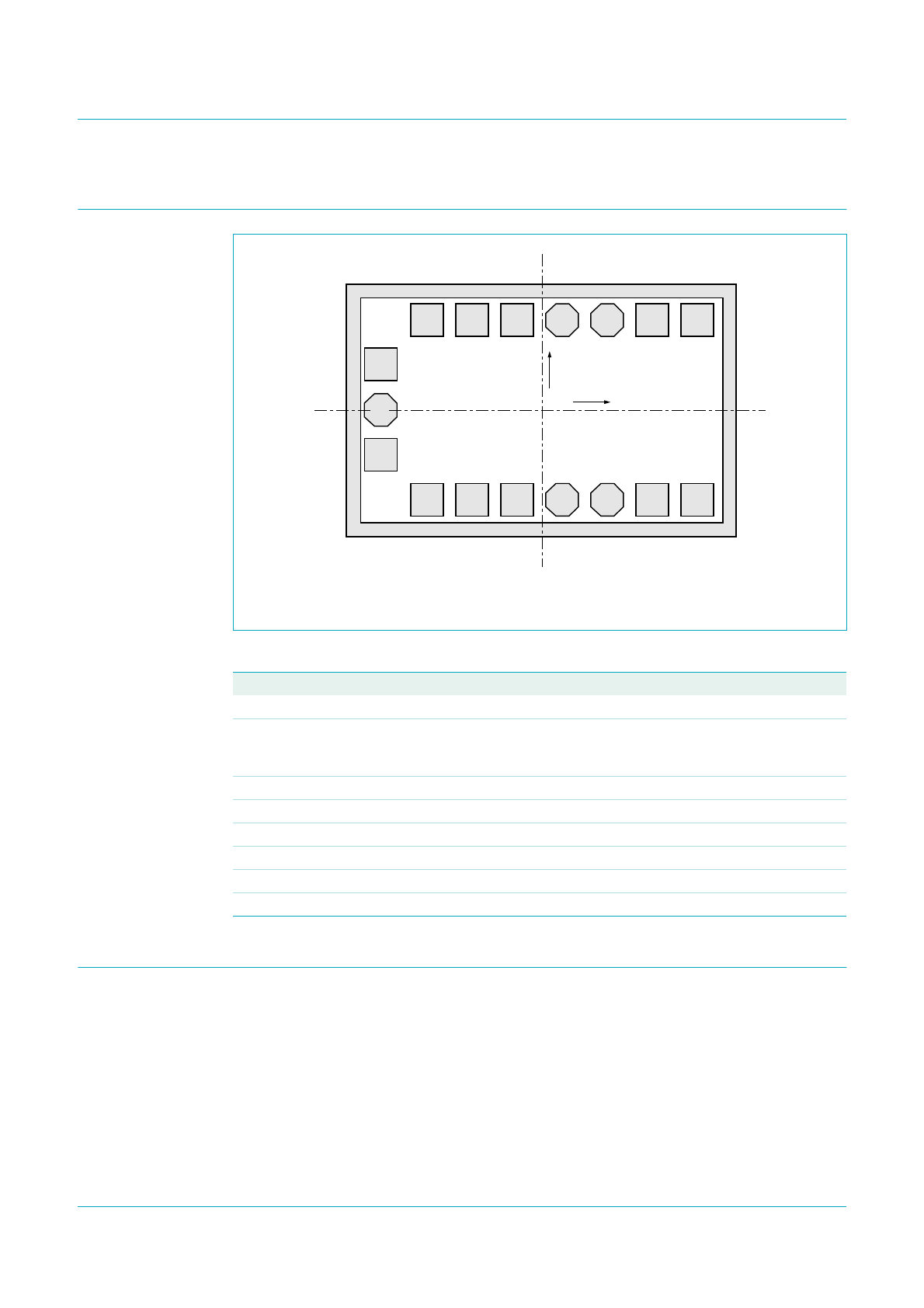
12. Bare die information
13. Package outline
Not applicable.
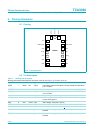
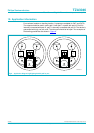
Origin is center of die.
Fig 10. Bonding pad locations
Table 5: Physical characteristics of the bare die
Parameter Value
Glass passivation 0.3 µm PSG (PhosphoSilicate Glass) on top of 0.8 µm silicon nitride
Bonding pad
dimension
minimum dimension of exposed metallization is 90 µm × 90 µm
(pad size = 100 µm × 100 µm) except pads 2 and 3 which have exposed
metallization of 80 µm × 80 µm (pad size = 90 µm × 90 µm)
Metallization 2.8 µm AlCu
Thickness 380 µm nominal
Die dimension 820 µm × 1300 µm (± 20 µm
2
)
Backing silicon; electrically connected to GND potential through substrate contacts
Attach temperature < 440 °C; recommended die attach is glue
Attach time < 15 s
456
(0,0)
X
Y
17 16 15 14 13 12 11
78910
001aac627
1
2
3