


TZA3046_1 © Koninklijke Philips Electronics N.V. 2006. All rights reserved.
Product data sheet Rev. 01 — 19 May 2006 4 of 15
Philips Semiconductors
TZA3046
Fiber Channel/Gigabit Ethernet transimpedance amplifier
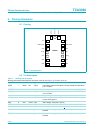
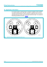
[1] These pads go HIGH when current flows into pad IPHOTO.
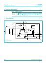
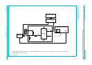
7. Functional description
The TZA3046 is a TransImpedance Amplifier (TIA) intended for use in fiber optic receivers
for signal recovery in FC/GE or FTTx applications. It amplifies the current generated by a
photo detector (PIN diode or avalanche photodiode) and converts it to a differential output
voltage.
The most important characteristics of the TZA3046 are high receiver sensitivity, wide
dynamic range and large bandwidth. Excellent receiver sensitivity is achieved by
minimizing transimpedance amplifier noise.
The TZA3046 has a wide dynamic range to handle the signal current generated by the
PIN diode which can vary from 2.5 µA to 1.7 mA (p-p). This is implemented by an AGC
loop which reduces the preamplifier feedback resistance so that the amplifier remains
linear over the whole input range. The AGC loop hold capacitor is integrated on-chip, so
an external capacitor is not required.
The bandwidth of TZA3046 is optimized for FC/GE application. It works from DC onward
due to the absence of offset control loops. Therefore the amount of Consecutive Identical
Digits (CID) will not effect the output waveform. A differential amplifier converts the output
of the preamplifier to a differential voltage.
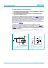
7.1 PIN diode connections
The performance of an optical receiver is largely determined by the combined effect of the
transimpedance amplifier and the PIN diode. In particular, the method used to connect the
PIN diode to the input (pad IPHOTO) and the layout around the input pad strongly
influences the main parameters of a transimpedance amplifier, such as sensitivity,
bandwidth, and PSRR.
Sensitivity is most affected by the value of the total capacitance at the input pad.
Therefore, to obtain the highest possible sensitivity the total capacitance should be as low
as possible.
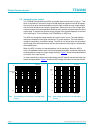
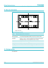
GND 11 486.4 278.6 ground ground; connect together pads 9, 10, 11 and pad 12 as many as
possible
GND 12 346.4 278.6 ground ground; connect together pads 9, 10, 11 and pad 12 as many as
possible
OUTQ 13 206.4 278.6 output data output; complement of pad OUT; use pad 7 or pad 13
OUT 14 66.4 278.6 output data output; use pad 8 or pad 14
[1]
AGC 15 −73.6 278.6 input AGC voltage; use pad 6 or pad 15
IDREF_MON 16 −213.6 278.6 output current output for RSSI measurements; connect a resistor to pad 5
or pad 16 and ground
V
CC
17 −353.6 278.6 supply supply voltage; connect supply voltage to pad 4 or pad 17
Table 2: Bonding pad description
…continued
Bonding pad locations with respect to the center of the die (see Figure 10); X and Y are in
µ
m.
Symbol Pad X Y Type Description