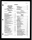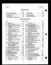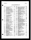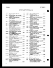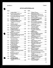
contents
HP 8673C/D
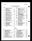
LIST OF ILLUSTRATIONS (cont’d)
Figure
Page
8.284. A5A2A2 D&&x Board Assembly
Component and Teat Pcdnt
Location . .8-281
8.285. Detector Assembly
Schematic Diagram t*t*tt * ttt*ttttt ..8-281
8-286. ASAl Front Panel Assembly
Component Location . . .8-283
8-287. A5 Front Panel Board Assembly
Schematic Diagram . . .8-283
8-288. ASA Switch Driver Assembly
Component and Test Point
Location . . .‘. .8-285
8-289. Switch Driver Board Assembly
Schematic Diagram . .8-285
8.290. A5A.3 Function Board Assembly
component and Teat Point
Location .8-287
8-291. A5 Function Board Assembly
Schematic Diageram
. . . . . . . . . . . . . . ...8-267
8-292. ASA Microprocessor Assembly
Component and Test Point
Location . .8-289
8-293. A5 Microprocessor Assembly
Schematic Diagram .8-289
8-294. A5A5 DAC and Enable Assembly
Component and Test Point
Location . . . . .8-291
8-295. A5 DAC and Enable Assembly
Schematic Diagram .8-291
8-296. Low Band RF Chain
Component Location
. . . . . . . . . . . . . . ...6-293
8.297. Low Band RF Chain
Schematic Diagram .8-293
8-298. A5AlO Power Supply Assembly
Component and Test Point
Location . * * .a-295
Figure
a-299.
8-300.
8-301.
8.302.
8.303.
8.304.
e-305.
5306.
8.307.
8.308.
S-309.
8.310.
8-311.
8.312.
8-313.
8-314.
8.315.
8316.
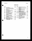
TABLES
Table Page Table
Page
+28V, +ZOV, and +15V Power Supply
Schematic. .8-295
A5A10 Power Supply Assembly
Component and Test Point
Location .8-297
+5V, -1OV, and -40V Power Supply
Schematic Diagram ;. .8-297
wnit Separation
. . . . . . . . . . . . . . . . . . . . . ...8-298
A3 Transformer and Filter Capacitor
Rsmover . . . . . . . . . . . . . . . . . . . . . . . . . . ...8-800
Al RF Output Assembly -
YTM Relays and Attenuator .8301
Al RF Output Assembly -
Pre Amp and Power Amp . .8-302
Location of YTO Mounting Screws .8-302
YTO Loop in Service Position .8-502
A5 Card Cage and Processor
Board in Service Position . . .8-303
A5 Power Transformers .8-303
Top View, Upper Unit Component
Location x305
Top View, Upper Unit DCU and
RF Covers Removed -
component Locatioion * * . . * . .8.305
Top View, Upper Unit,
Test Point Location,. . , . , . , .8-305
Bottom View, Upper Unit,
Component Location . . .8-SO5
Bottom View, Lower Unit Teat Point
and Component Location .8-307
Bottom View, Lower Unit
Component Locations , , , , , *. , t , , , . .8307
Top View, Lower Unit -
Component Location . .8-307
Page
6-l.
5-2.
6-3.
6-4.
6-l.
6-2.
63.
6-4.
8-l.
8-2.
8-3.
8-4.
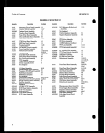
Factory Selected Components .............. .5-4
Performance Test Failure and
Required Action .......................... .5-5
PoshRepair Adjustments ................... .5-6
YTF Band Adjustments ................... ,549
Part Numbers for Exchange Assemblies .... .6-2
Reference Designations and
Abbreviations. ........................... .6-3
Replaceable Parts .......................... .65
Code List of Manufacturers ............... .6-106
Schematic Diagram Notes .................. .8-4
Service Functions ......................... .8-12
Etched Circuit Soldering Equipment ....... .8-16
Front Panel Status Annunciators ........... S-34
8.5. Listing of All M and N Numbers and
Resulting Frequencies ................... ,8-46
8.6. LFS lK-8M Inputs ....................... .&52
8.7. LFS 1K--8M Inputs ....................... .8-52
8.8. Ml-M6 and Nl-N5 Inputs .................. .8-54
8.9. Ml-M6 and Nl-N5 Outputs ................ .&54
8.10. DAC! 1.4800 MHz Inputs ................... ,856
8.11. DAC l-4800 MHz Outputs ................. ,856
8.12. Band Numbers and Frequencies ........... ,868
8.13. SRD Bias Voltages ........................ ,860
8.14. HP 8673C Power Failure Modes. ........... .8-64
8-15. BP 8673D Power Failure Modes ........... .8-65
8.16. Switch Driver ASAB Checka ............... ,846
8.17. Switch Driver Checkout ................... .8S7


