HP 86732/D
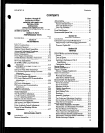
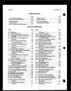
Contents
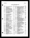
LIST OF ILLJJSTRATIONS (cont’d)
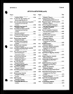
Figure
8-238.
8.239.
8.240.
8.241.
8-242.
8.243.
8-244.
8-245.
8-246.
8-247.
8-248.
8.249.
8.250.
8-251.
8.252.
8.253.
8.254.
8.255.
8-256.
8.257.
8.258.
8.259,
8.260.
Page
RF Filter Circuits Component
Location (867311) .8-236
P/O RF Filter, RF Amplifier, and
Detector Amplifier Circuits
(See also Figure 8-237) .8-237
AlAl Attenuator Driver Board Assembly
Component and Test Point
Location .8-239
Attenuator Driver Assembly
Schematic Diagram .8-239
AlA SRD Bias Board Assembly
Component and Test Point
Location .8-241
SRD Control Assembly
Schematic Diagram . .8-241
AlA. Function Board Aaeembly
Component and Test Point
Location .8-243
Function Board Assembly
Schematic Diagram .8-243
AlA Meter Board Assembly
Component and Test Point
tocation J-245
Metering Control Assembly
Schematic Diagram .8-245
AlAS DAC and Enable Board Assembly
Component and Test Point
Location .8-247
DAC and Enable Assembly
Schematic Diagram .8-241
P/O A4Al Front Panel Assembly
component Lo ti ca on .8-249
A4 Front Panel Keyboard
Schematic Diagram .8-249
A2A2 Key Code Assembly
Component Location .8-251
Key Code Assembly
Schematic Diagram , t t , . .8-251
A2A1 Panel Driver Assembly
Component Location t .8-253
Panel Driver Assembly
Schematic Diagram .8-253
A2A8 Microprocessor Board Assembly
Component and Teat Point
Location
t t t t t t .8-255
Microprocessor Assembly
Schematic Diagram .8-255
A2All Ilom Assembly Component
Location .&257
ROM Assembly
Schematic Diagram *. t .&257
A2AlO RAM Assembly
Component and Test Point
Location t t .8-259
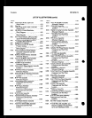
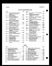
Figure
8-261.
8-262.
8-263.
8-264.
8-265.
8-266.
8.267.
8-268.
8.269.
8.270.
8-271.
8.272.
8.273.
8-274.
8-275.
8-276.
8-277.
8-278.
8.279.
8.280.
8-281.
8.282.
8283.
Page
RAM Assembly
Schematic Diagram .8-259
A2A9
Frequency Output -
HP-IB Assembly Component and
Test Point Location. , .8.261
Frequency Output - HP-IB Assembly
Schematic Diagram .8-261
A2A7 I/O Assembly Component
and Test Point Lwation, Part 1 .8-263
I/O Assembly Schematic
Diagram, Part 1 .8-263
A2A7 I/O Assembly Component
and Teat Point Location, Part 2 .8-265
I/O Assembly Schematic
Diagram, Part 2 .8-265
A4Al Front Panel Assembly
Component Location .8-267
A4 Front Panel Display
Schematic Diagram , .8-267
A3Al Rectitkr Assembly
Component and Test Point
Location . . . . . . . . . . . . . . . . . . . . . . . . . . ...8-269
Rectifier Assembly
Schematic Diagram *. , .8-269
A3A.3 Positive Regulator Assembly
Component and Test Point
Location . , .a-271
Positive Regulator Assembly
Schematic Diagram .8-271
A3A4 Negative Regulator Assembly
Component and Test Point
Location . . .8-273
Negative Regulator Assembly
Schematic Diagram ,8-273
ASA Detectcr/ALC Assembly
Component and Test Point
Location t t .8-274
A5A6 Switch Driver Assembly
Component and Teet Point
Location t , t , .8-274
Detector/ALC Assembly
Schematic Diagram , t , .8-275
A5A18Al Pulse Input Switch Board
Assembly Component Location .8-276
A5A4 Pulse Driver Processing Assembly
Component and Test Point
Location t . t t t t .8-276
Pulse Driver Processing Assembly
Schematic Diagram , t , , .8-277
A5A7 YIG Driver Board Assembly
Component and Teat Point
Location . , I , , , .8-279
A5 YIG Driver Assembly
Schematic Diagram t , .8-279
vii


