


3. Check for proper operation of the synthesizer. There
should be approximately 0 dBm drive level on the
SYNTH output line for proper transmit operation. If
a Syntheiszer problem is suspected, following the
suggestions in Troubleshooting Synthesizer section.
4. If current consumption appears normal, and the syn-
thesizer output level is correct, check that the DPTT
and BAND SW lines are in the proper state. The
problem may be in the antenna T/R switch circuit
with diodes D101, D102 or in the antenna connector
W1. A problem in the antenna switch circuit or the
antenna connector may also cause the receiver to be
weak.
5. If the synthesizer drive level seems normal, but cur-
rent consumption is low, the transistor stages in the
transmitter RF chain should next be checked, begin-
ning with the final amplifier Q105.
Transmit Audio Problem
1. For a transmit audio problem the trouble could be
either in the Syntheiszer Board or the T/R Board.
Monitoring the TX MOD line for correct audio
should identify which.
2. If the problem seems to be on the T/R Board, then try
the following steps:
a. Check to see if the MIC output is reaching the
T/R Board.
b. Check to see if the audio is present at the pre-
amplifier output, collector of Q301.
c. Check to see if the audio is present at the audio
limiter output, U301-D pin 14.
d. Check to see if the MIC MUTE line is in the
proper state, low for not muted.
e. Check that the
PTT is arriving at the microproc-
essor U701 pin 7. This is the command to gen-
erate the DPTT and BAND SW signals along
with the MIC MUTE signal.
3. If Channel Guard is to be transmitted, then:
a. Check to see if Channel Guard is being gener-
ated at CG ENC output by microprocessor
switching outputs U701 pins 34-37.
b. Check to see if the Channel Guard signal is at
the output of the Tx Channel Guard low pass
filter U603-A pin 1.
c.
Check to see that Channel Guard signal is at the
output of the post limiter filter, U301-A pin 1, or
at the TX MOD output.
4. If the TX MOD output is proper from the T/R Board,
then check to see if the audio signal is arriving at the
Synthesizer Board. If so, on the Synthesizer Board:
a. Check to see if the audio is at Mod Pot R230 pin
1.
b. Check to see if the audio level at the centertap of
Mod Pot R230 changes with pot setting.
c. Check that the audio signal is arriving at the
VCO U204 pin 3.
RECEIVER
Receiver problems will generally only be found on the
T/R Board, in the following sectors:
• Receiver RF circuitry beginning at antenna jack J3
• Receiver IF circuitry, 45 MHz 1st IF and 455 kHz
2nd IF
• Source of audio signals beginning at the quadrature
detector output in U501
• Three paths of audio processing beginning with the
VOL SQ HI signal:
1. Voice path, through to the speaker output
2. Squelch noise path, through to
CAS output
3. Tone data path, through TN DATA output
• Microprocessor and circuitry controlled by it, in-
cluding synthesizer
• Speaker, at final output
Receive Audio Problem, Low Audio Level Or No
Audio
The following steps are suggested to locate the trouble:
1. Be sure the programming is correct.
2. Check to see if the receiver is unsquelched with strong
on-channel signal:
CAS is low, as controlled by SQ
POT R619.
3. Check the RX MUTE and
MUTE gates are in correct
states.
4. In the voice path check that audio is reaching the output
stage U602-B pin 7, and its output on pin 1.
5. Check that power is applied to audio amplifier U602-B
pin 2.
6. Check that audio is reaching the speaker through the
Accessory Jack Board.
7. Check that when channel guard is used the tones are
found on the TN DATA line. When T99 tones are used
they should be at TN DATA.
8. Check that data reaches the microprocessor, and that
the receiver is unmuted when correct limited tone chan-
nel guard data or correct Type 99 tones are decoded.
9. If digital channel guard is being used, check to see if
the polarity is correct.
Receiver Sensitivity Problem
1. Check that 5.4 V, RX 5.4 V, SYNTH 5.4 V, and VREF
are present where indicated.
2. Check to see if the antenna clip W1 is soldered to the
center pin of BNC antenna connector J3.
3. Check that DC voltages in the RF stages are correct.
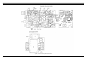
(Refer to the schematic diagram in LBI-38555).
4. Check that RF gains are correct. (Refer to Block Dia-
gram in LBI-38555).
5. Check to see if the first and second LO injection fre-
quencies are correct.
6. Check for proper LO injection signal levels.
7. Check to see if the quadrature detector is tuned for
maximum audio output level at the speaker when an
input RF signal is modulated with a 1 kHz tone at 3 kHz
peak deviation.
8. If a sensitivity problem or a distortion problem remains,
then a receiver RF and IF alignment should be done
using the recommended procedures in the alignment
section.
Receiver Squelch Problem
1. Check for presence of noise at VOL SQ HI line when
no received RF carrier is present.
2. In the squelch noise path check for presence of filtered
noise at output of high pass filter U501 pin 11.
3. Check to see if the noise level at U501-11 decreases
when a RF signal is input to the receiver.
4. With no carrier, be sure noise is present at pin 1 of
squelch pot R619, and also at U603 pin 12 when
squelch pot is rotated.
5. Check that the DC level of the filtered noise output
measured at U603-B pin 6 varies with RF signal level.
6. Make certain that a threshold voltage is present at
comparator input U603-B pin 5.
7. Check to see if the
CAS line switches low when a RF
signal carrier is introduced.
8. Check that the DC level at the threshold terminal U603-
B pin 5 increases when the voltage of the
CAS line
increases.
9. Make certain that the
CAS line switching voltage
reaches the microprocessor input U701 pin 13.
SYNTHESIZER
Troubleshooting the synthesizer circuit consists of first
checking for the proper D.C. levels. Then determing if proper
waveforms are present and checking individual modules.
When the channel switch or the
PTT switch is operated, the
SYN ENABLE, SYN DATA and SYN CLK should become
active. Monitor these lines and troubleshoot the Transmit/Re-
ceive Board if activity does not occur.
TX Modulation
Check to see if the audio is at pin 1 of the Mod Pot R230.
The audio level at pin 2 of the Mod Pot should change when
the pot is rotated. Finally, check to see if the audio signal is
arriving at pin 5 at U206.
NOTE
To facilitate testing of receiver problems, the bat-
tery saver mode can be disabled by shorting the
TEST input to the microprocessor to ground during
power-up. The radio can be taken out of test mode
by recycling the power without TEST grounded.
LBI-38557 LBI-38557
6